8
Servicing method
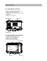
4.11. Removing the LCD panel.
1. Remove the Shield pcb assy.(See 5.10.)
2. Remove the fixing screws(4pcs).
3. Disconnect the coupler (A5), (B1), (B2),
(B3), (B4).
4. Remove the LCD panel.
4.12. Removing the A-board, B-board.
1. Remove the LCD panel.(See 5.11.)
2. Remove the fixing screws(8pcs).
3. Disconnect the coupler(A6).
4. Remove the A-board, B-board.
Coupler(B1),(B2)
Coupler(B3),(B4)
Coupler(A5)
Coupler(A6)
B-board
A-board
Summary of Contents for Viera TX-17LX2
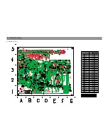
Page 12: ...11 Conductor Views 6 2 MAIN PCB BOTTOM...
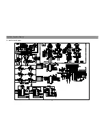
Page 14: ...13 Block and Schematic Diagrams 7 2 Signal Block Diagram...
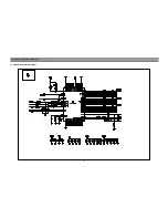
Page 15: ...14 Block and Schematic Diagrams 7 3 Power Schematic Diagram...
Page 16: ...15 Block and Schematic Diagrams 7 4 VCTI Schematic Diagram...
Page 17: ...16 Block and Schematic Diagrams 7 5 Input Schematic Diagram...
Page 18: ...17 Block and Schematic Diagrams 7 6 Memory AMP Schematic Diagram...
Page 19: ...18 Block and Schematic Diagrams 7 7 AD9883 Schematic Diagram...
Page 20: ...19 Block and Schematic Diagrams 7 8 Deinterlace Schematic Diagram...
Page 21: ...20 Block and Schematic Diagrams 7 9 SDRAM Schematic Diagram...
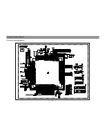
Page 22: ...21 Block and Schematic Diagrams 7 10 Image Processor Schematic Diagram...
Page 23: ...22 Block and Schematic Diagrams 7 11 LVDS KEY Schematic Diagram...
Page 25: ...24 Parts Location Mechanical Replacement Parts List 8 2 Packing Exploded View...

