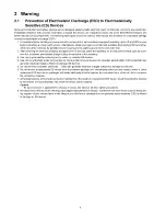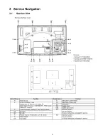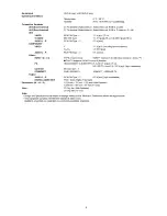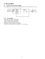
2 Warning
2.1.
Prevention of Electrostatic Discharge (ESD) to Electrostatically
Sensitive (ES) Devices
Some sem iconductor (solid state) devices can be damaged easily by static electricity. Such components commonly are called Elec
trostatically Sensitive (ES) Devices. Examples of typical ES devices are integrated circuits and some field-effect transistors and
sem iconductor [chip] components. The following techniques should be used to help reduce the incidence of com ponent damage
caused by electrostatic discharge (ESD).
1. Immediately before handling any sem iconductor com ponent or semiconductor-equipped assembly, drain off any ESD on your
body by touching a known earth ground. Alternatively, obtain and w ear a com m ercially available discharging ESD w rist strap,
which should be removed for potential shock reasons prior to applying power to the unit under test.
2. A fter removing an electrical assembly equipped with ES devices, place the assembly on a conductive surface such as alumi
num foil, to prevent electrostatic charge buildup or exposure of the assembly.
3. Use only a grounded-tip soldering iron to solder or unsolder ES devices.
4. Use only an anti-static solder removal device. Some solder removal devices not classified as [anti-static (ESD protected)] can
generate electrical charge sufficient to damage ES devices.
5. Do not use freon-propelled chemicals. These can generate electrical charges sufficient to damage ES devices.
6. Do not remove a replacement ES device from its protective package until immediately before you are ready to install it. (Most
replacement ES devices are packaged with leads electrically shorted together by conductive foam, aluminum foil or compara
ble conductive material).
7. Immediately before removing the protective material from the leads of a replacement ES device, touch the protective material
to the chassis or circuit assembly into which the device will be installed.
Caution
Be sure no power is applied to the chassis or circuit, and observe all other safety precautions.
8. Minimize bodily motions when handling unpackaged replacement ES devices. (Otherwise ham less motion such as the brush
ing together of your clothes fabric or the lifting of your foot from a carpeted floor can generate static electricity (ESD) sufficient
to damage an ES device).
4
Summary of Contents for Viera TX-P42G15E
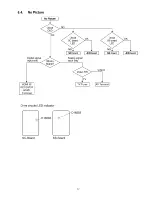
Page 17: ...6 4 No Picture No Picture Check NG 17...
Page 31: ...9 1 4 9 1 5 Adjustment Volume Location Test Point Location 31...
Page 36: ...36...
Page 37: ...10 Block Diagram 10 1 Main Block Diagram 3 D IG IT A L S IG N A L P R O C E S S O R 37...
Page 38: ...10 2 Block 1 5 Diagram 38 0 0...
Page 40: ...10 4 Block 3 5 Diagram F O R M A T C O N V P L A S M A AI FOR FACTORY USE 40...
Page 44: ...11 3 Wiring 2 44...
Page 45: ...11 4 Wiring 3 45...
Page 46: ...U U U U D i 11 5 Wiring 4 46...
Page 47: ...11 6 Wiring 5 47...
Page 48: ...11 7 Wiring 6 48...
Page 49: ...11 8 Wiring 7 49...
Page 50: ...50...
Page 51: ...11 10 Wiring 9 51...
Page 52: ...52...
Page 55: ...12 2 P Board 1 2 Schematic Diagram A B C D E F 1 2 3 4 5 6 7 54...
Page 56: ...12 3 P Board 2 2 Schematic Diagram 55...
Page 60: ...12 7 A Board 3 22 Schematic Diagram IC 8002 MN2WS0058 19 2 0 21 2 2...
Page 64: ...V 42 43 44 45...
Page 66: ...A BO AR D 6 22 P e a ks M O D E L R EF N o 8 0 0 0 8 9 9 9 TO 5 22 TO 5 16 22 5 1 53 54...
Page 72: ...67...
Page 74: ...105 106 107 108...
Page 76: ...5 I AVSW5V1 113 114 115 116 117 69...
Page 78: ...V ID E O DET V ID E O IN 122 123 124 125 126 70...
Page 80: ...131 132 133 134 135 71...
Page 84: ...158 159 160 161 162 74...
Page 88: ...STB3 3V Q5431 185 186 187 188 189 77...
Page 90: ...SUB6v IC 2802 194 195 196 197 198 78...
Page 91: ...12 27 D Board 1 4 Schematic Diagram 79...
Page 92: ...12 28 D Board 2 4 Schematic Diagram 80...
Page 95: ...12 31 C1 Board 1 2 Schematic Diagram D A C1 BOARD TNPA4762 1 2 1 2 3 4...
Page 96: ...PANEL DATA DRIVER 5 1 6 1 7 1 8 1 9 83...
Page 101: ...12 36 SC Board 2 4 Schematic Diagram 10 11 12 13 14 15 16 17 18 88...
Page 102: ...12 37 SC Board 3 4 Schematic Diagram 19 1 20 1 21 1 22 1 23 1 24 1 25 1 26 1 27 89 C D...
Page 103: ...12 38 SC Board 4 4 Schematic Diagram 28 29 30 31 32 33 34 35 36 90...
Page 110: ...P BOARD COMPONENT SIDE ETX2MM747MFF 6 5 4 3 2 1 A I B I C I D I E I F I G I H I I 95...
Page 117: ...D BOARD COMPONENT SIDE TZTNP02DTUE 101...
Page 121: ...13 8 SC Board SC BOARD FOIL SIDE TNPA4844AH A D...
Page 122: ...104...
Page 125: ...6 SC BOARD COMPONENT SIDE TNPA4844AH 5 4 3 2 1 A I B I C I D I E I F I G I H I I 106...
Page 129: ...14 1 2 Packing 1 110...
Page 130: ...111...


