6.2.
Option - Mirror
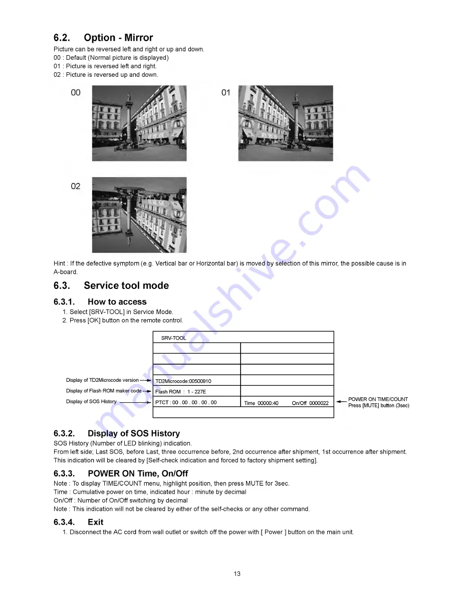
Picture can be reversed left and right or up and down.
00
01
02
Default (Normal picture is displayed)
Picture is reversed left and right.
Picture is reversed up and down.
Hint : If the defective symptom (e.g. Vertical bar or Horizontal bar) is moved by selection of this mirror, the possible cause is in
A-board.
6.3.
Service tool mode
6.3.1.
How to access
1. Select [SRV-TOOL] in Service Mode.
2. Press [OK] button on the remote control.
Display of TD2Microcode version —
Display of Flash ROM maker code -
Display of SOS History ----------------
SRV-TOOL
TD2Microcode:00500910
Flash ROM : 1 - 227E
PTCT : 00 . 00 . 00 . 00 . 00
Time 00000:40
On/Off 0000022
. POWER ON TIME/COUNT
Press [MUTE] button (3sec)
6.3.2.
Display of SOS History
SOS History (Number of LED blinking) indication.
From left side; Last SOS, before Last, three occurrence before, 2nd occurrence after shipment, 1 st occurrence after shipment.
This indication will be cleared by [Self-check indication and forced to factory shipment setting].
6.3.3.
POWER ON Time, On/Off
Note : To display TIME/COUNT menu, highlight position, then press MUTE for 3sec.
Time : Cumulative power on time, indicated hour : minute by decimal
On/Off : Number of On/Off switching by decimal
Note : This indication will not be cleared by either of the self-checks or any other command.
6.3.4.
Exit
1. Disconnect the AC cord from wall outlet or switch off the power with [ Power ] button on the main unit.
13
Summary of Contents for Viera TX-P42U20B
Page 21: ...7 4 No Picture 21...
Page 33: ...11 Block Diagram 11 1 Main Block Diagram 33...
Page 34: ...11 2 Block 1 4 Diagram 34...
Page 35: ...G 0 11 3 Block 2 4 Diagram I A I D IG IT A L S IG N A L P R O C E S S O R 35...
Page 36: ...11 4 Block 3 4 Diagram P P O W E R S U P P LY 36...
Page 38: ...38...
Page 40: ...12 3 Wiring 2 40...
Page 43: ...13 2 P Board 1 4 Schematic Diagram A B C D E A P BO ARD LSEP1287BE HB 1 4 F 1 2 3 4 42...
Page 44: ...13 3 P Board 2 4 Schematic Diagram A P BO ARD LSEP1287BE HB 2 4 10 11 12 13 14 15 16 17 18 43...
Page 45: ...13 4 P Board 3 4 Schematic Diagram A B C D E F 1 2 3 4 44 5...
Page 46: ...13 5 P Board 4 4 Schematic Diagram 10 11 12 13 14 15 16 17 18 45...
Page 47: ...13 6 A Board 1 19 Schematic Diagram A A A BO AR D 1 19 IIC B C D E F 1 2 3 4 9 46...
Page 52: ...13 11 Board 6 19 Schematic Diagram A A BO AR D 6 19 STB MPU 46 47 48 49...
Page 54: ...13 12 Board 7 19 Schematic Diagram A A BO AR D 7 1 9 HDMI 55 56 57 58 59 52...
Page 55: ...60 61 62 63...
Page 57: ...69 70 71 72...
Page 60: ...87 8 8 89 90...
Page 61: ...13 16 A Board 11 19 Schematic Diagram A A BO AR D 11 19 A V SW 91 92 93 94 95 96 97 98 99 56...
Page 63: ...FE_Virtual_M odule Peaks COMMON TO 3 19 Analog ASIC 104 105 106 107 108 57...
Page 68: ...140 141 142 143 144 61...
Page 71: ...63...
Page 72: ...13 24 A Board 19 19 Schematic Diagram A A BO AR D 19 19 DVB T C D EM O D U LATO R 64...
Page 75: ...13 27 C2 Board 1 2 Schematic Diagram A A C 2 BO AR D TN PA5095 1 2 ___ I TO A BOARD A32 B 67...
Page 78: ...13 30 SC Board 2 4 Schematic Diagram 10 I 11 1 12 1 13 1 14 1 15 1 16 1 17 1 18 70...
Page 79: ...13 31 SC Board 3 4 Schematic Diagram 19 1 20 1 21 1 22 1 23 1 24 1 25 1 26 1 27 71...
Page 80: ...13 32 SC Board 4 4 Schematic Diagram 28 29 30 31 32 33 34 35 36 72...
Page 86: ...P BOARD COMPONENT SIDE LSEP1287BEHB B G 6 5 4 3 2 1 E F H 77...
Page 88: ...14 3 A Board 79...
Page 89: ...A BOARD COMPONENT SIDE A P42U20B A P42U20E A PR42U20 B G 6 5 4 3 2 1 E F H 80...
Page 92: ...14 6 SC Board SC BOARD FOIL SIDE TXNSC11DEK B G 6 5 4 3 2 1 E F H 83...
Page 93: ...SC BOARD COMPONENT SIDE TXNSC11DEK 6 5 4 3 2 1 A I b I C I d I E I F I G I H I I 84...
Page 94: ...14 7 SS Board SS BOARD FOIL SIDE TXNSS11DEK 6 5 4 3 2 1 A I b I C I d I E I F I G I H I I 85...
Page 95: ...SS BOARD COMPONENT SIDE TXNSS11DEK...
Page 96: ......
Page 98: ...15 1 2 Exploded View 2 88...
Page 99: ...89...
Page 100: ...15 1 4 Packing 2 90...


