background image

17

6.2.

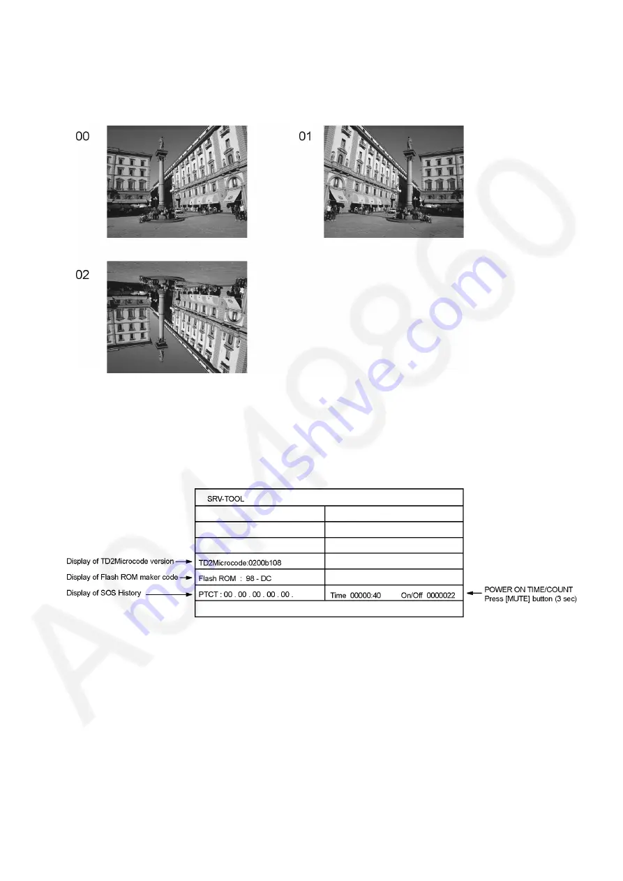
Option - Mirror

Picture can be reversed left and right or up and down.
00 : Default (Normal picture is displayed)
01 : Picture is reversed left and right.
02 : Picture is reversed up and down.

Hint : If the defective symptom (e.g. Vertical bar or Horizontal bar) is moved by selection of this mirror, the possible cause is in 
A-board. 

6.3.

Service tool mode

6.3.1.

How to access 

1. Select [SRV-TOOL] in Service Mode.
2. Press [OK] button on the remote control.

6.3.2.

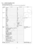
Display of SOS History

SOS History (Number of LED blinking) indication.
From left side; Last SOS, before Last, three occurrence before, 2nd occurrence after shipment, 1st occurrence after shipment.
This indication will be cleared by [Self-check indication and forced to factory shipment setting].

6.3.3.

POWER ON Time, On/Off

Note : To display TIME/COUNT menu, highlight position, then press MUTE for 3 sec.
Time : Cumulative power on time, indicated hour : minute by decimal
On/Off : Number of On/Off switching by decimal
Note : This indication will not be cleared by either of the self-checks or any other command.

6.3.4.

Exit

1. Disconnect the AC cord from wall outlet or switch off the power with [ Power ] button on the main unit.

Summary of Contents for Viera TX-P50VT50B

Page 1: ... Panasonic Corporation 2012 Unauthorized copying and distribution is a violation of law ORDER NO PCZ1204080CE Plasma Television Model No TX P50VT50B TX P50VT50Y TX PR50VT50 GPF15D E Chassis ...

Page 2: ...ool mode 17 6 4 DRV Check USBHDD Check 18 6 5 Hotel mode 18 6 6 Data Copy by SD Card 19 7 Troubleshooting Guide 22 7 1 Check of the IIC bus lines 22 7 2 Power LED Blinking timing chart 23 7 3 No Power 24 7 4 No Picture 25 7 5 Local screen failure 26 8 Service Fixture Tools 27 8 1 SC jig 27 9 Disassembly and Assembly Instructions 28 9 1 Disassembly Flow Chart for the Unit 28 9 2 Disassembly Procedu...

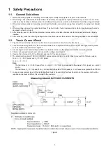
Page 3: ... 1 2 Touch Current Check 1 Plug the AC cord directly into the AC outlet Do not use an isolation transformer for this check 2 Connect a measuring network for touch currents between each exposed metallic part on the set and a good earth ground such as a water pipe as shown in Figure 1 3 Use Leakage Current Tester Simpson 228 or equivalent to measure the potential across the measuring network 4 Check...

Page 4: ... of the assembly 3 Use only a grounded tip soldering iron to solder or unsolder ES devices 4 Use only an anti static solder removal device Some solder removal devices not classified as anti static ESD protected can generate electrical charge sufficient to damage ES devices 5 Do not use freon propelled chemicals These can generate electrical charges sufficient to damage ES devices 6 Do not remove a...

Page 5: ...ee solder has a higher melting point than standard solder Typically the melting point is 50 70 F 30 40 C higher Please use a high temperature soldering iron and set it to 700 20 F 370 10 C Pb free solder will tend to splash when heated too high about 1100 F or 600 C If you must use Pb solder please completely remove all of the Pb free solder on the pins or solder area before applying Pb solder If ...

Page 6: ...nput processing K Remote receiver Power LED C A T S sensor C1 Data Driver Lower Right C2 Data Driver Lower Center C3 Data Driver Lower Left SC Scan Drive SS Sustain Drive SS2 Sustain out Lower SU Scan out Upper Non serviceable SU Board should be exchanged for service SD Scan out Lower Non serviceable SD Board should be exchanged for service ...

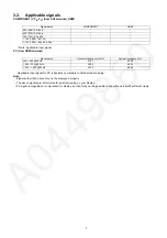
Page 7: ... The above signals are reformatted for optimal viewing on your display PC signal is magnified or compressed for display so that it may not be possible to show fine detail with sufficient clarity Signal name COMPONENT HDMI 525 480 60i 60p 625 576 50i 50p 750 720 60p 50p 1 125 1 080 60i 50i 1 125 1 080 60p 50p 24p Signal name Horizontal frequency kHz Vertical frequency Hz 640 480 60 Hz 31 47 60 00 1...

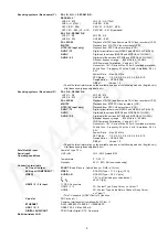
Page 8: ... MS s FEC Mode 1 2 3 5 2 3 3 4 4 5 5 6 8 9 9 10 Demodulation QPSK 8PSK Not available for DiSEqC control DVB T T2 Digital terrestrial services PAL I UHF E21 68 PAL 525 60 Playback of NTSC tape from some PAL Video recorders VCR or NTSC disc playback from DVD player and recorder M NTSC Playback from M NTSC Video recorders VCR NTSC AV input only Playback from NTSC Video recorders VCR Receiving systems...

Page 9: ... Playback from NTSC Video recorders VCR DVB T T2 Digital terrestrial services MPEG2 and MPEG4 AVC H 264 DVB C Digital cable services MPEG2 and MPEG4 AVC H 264 DVB S S2 Digital satellite services MPEG2 and MPEG4 AVC H 264 Receiver frequency range 950 MHz to 2 150 MHz LNB Power and Polarisation Vertical 13 V Horizontal 18 V Current Max 500 mA overload protection 22 kHz Tone Frequency 22 kHz 2 kHz Am...

Page 10: ...epending on the country 4 Not all the Bluetooth compatible devices are available with this TV Up to 5 devices can be used simultaneously except the 3D Eyewear and the VIERA Touch Pad Controller Dimensions W H D 167 7 mm 42 2 mm 170 7 mm Mass Approx 31 g Lens type Liquid Crystal Shutter Usage temperature range 0 C 40 C Battery Coin shaped lithium battery CR2025 Operation time Approx 75 hours in con...

Page 11: ...erate the final KEY data How to SELF CHECK While pressing VOLUME button on the main unit press MENU button on the remote control for more than 3 seconds TV will be forced to the factory shipment setting after this SELF CHECK 5 1 3 Model and Keys 5 2 USB HDD Recording 5 2 1 General information Digital TV programmes can be recorded in USB HDD A One to One key generated in A board by SELF CHECK binds...

Page 12: ...ameter signal does not need to be sent Please see other side regarding Commands and Parameters Connection Notes With standby mode this TV responds to PON and QPW commands only Wait for the response of the first command to come from this unit before sending the next command If multiple commands are transmitted be sure to keep intervals of 250 m sec Send the command again when the call back command ...

Page 13: ...D TVD DVB S Other Sat IMS BS1 BS1 Freesat IMS BS2 BS2 DVB C IMS CAB CAB Component 1 IMS C1 C1 Component2 IMS C2 C2 Video 1 IMS V1 V1 Video 2 IMS V2 V2 Video 3 IMS V3 V3 S Video 1 IMS S1 S1 SCART Cable S Video 2 IMS S2 S2 SCART Cable HDMI 1 IMS H1 H1 HDMI 2 IMS H2 H2 HDMI 3 IMS H3 H3 HDMI 4 IMS H4 H4 PC IMS PC PC SD photo viewer IMS SP SP VIERA CAST IMS VC VC PICTURE MODE Vivid Dynamic VPC VVT QPC ...

Page 14: ... QIF 480i 480p 576i 576p 720p 1080i 1080p DIRECT CH INPUT 0 ICH 0 1 ICH 1 2 ICH 2 3 ICH 3 4 ICH 4 5 ICH 5 6 ICH 6 7 ICH 7 8 ICH 8 9 ICH 9 MENU FUNCTION MENU MEN SELECT SEL RETURN RTN EXIT EXT ARROW LEFT ARL ARROW RIGHT ARR ARROW UP ARU ARROW DOWN ARD OPTION SUB MENU SUB RED RED GREEN GRN YELLOW YEL BLUE BLU VIERA TOOLS VTL ...

Page 15: ...e Mode 6 1 2 Key command 1 button Main items Selection in forward direction 2 button Main items Selection in reverse direction 3 button Sub items Selection in forward direction 4 button Sub items Selection in reverse direction RED button All Sub items Selection in reverse direction GREEN button All Sub items Selection in forward direction VOL button Value of sub items change in forward direction i...

Page 16: ...0 Y C Delay OPT 1 00110100 OPT 2 11101110 OPT 3 00000001 OPT 4 01010000 EDID CLK MID MIRROR 00 See Option Mirror AMR SELECT OFF VSUS LOW See Vsus selection AGING ALL WHITE Built in test patterns can be displayed MIDDLE BLUE WITH MAGENTA OUTSIDE FRAME MIDDLE STEP GREEN MIDDLE STEP RED LOW STEP WHITE ALL BLUE ALL GREEN ALL RED WHITE DIAGONAL STRIPE RED DIAGONAL STRIPE GREEN DIAGONAL STRIPE BLUE DIAG...

Page 17: ...History Number of LED blinking indication From left side Last SOS before Last three occurrence before 2nd occurrence after shipment 1st occurrence after shipment This indication will be cleared by Self check indication and forced to factory shipment setting 6 3 3 POWER ON Time On Off Note To display TIME COUNT menu highlight position then press MUTE for 3 sec Time Cumulative power on time indicate...

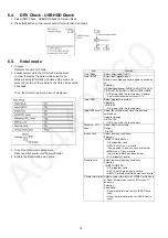
Page 18: ...iority to a last memory However Euro model is compulsorily set to TV Initial POS Select programme number Selection Off 0 to 99 Off give priority to a last memory Initial VOL Level Adjust the volume when each time power is switched on Selection Range Off 0 to 100 Off give priority to a last memory Maximum VOL Level Adjust maximum volume Range 0 to 100 Button Lock Select local key conditions Selecti...

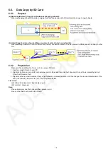
Page 19: ...Vs 6 6 2 Preparation Make pwd file as startup file for a or b in a empty SD card 1 Insert a empty SD card to your PC 2 Right click a blank area in a SD card window point to New and then click text document A new file is created by default New Text Document txt 3 Right click the new text document that you just created and select rename and then change the name and extension of the file to the follo...

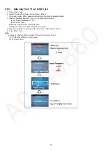
Page 20: ...llowing password for a or b by using remote control a For Board replacement 2770 b For Hotel 4850 Data will be copied from TV set to SD card It takes around 2 to 6 minutes maximum for copying 4 After the completion of copying to SD card remove SD card from TV set 5 Turn off the TV set Note Following new folder will be created in SD card for data from TV set a For Board replacement user_setup b For...

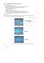
Page 21: ...nt 2771 b For Hotel 4851 Data will be copied from SD card to TV set 4 After the completion of copying to SD card remove SD card from TV set a For Board replacement Data will be deleted after copying Limited one copy b For Hotel Data will not be deleted and can be used for other TVs 5 Turn off the TV set Note 1 Depending on the failure of boards function of Data copy for board replacement does not ...

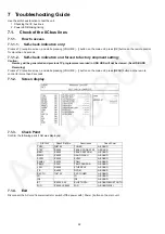
Page 22: ...ion screen and while pressing VOLUME button on the main unit press MENU button on the remote control for more than 3 seconds 7 1 2 Screen display 7 1 3 Check Point Confirm the following parts if NG was displayed 7 1 4 Exit Disconnect the AC cord from wall outlet or switch off the power with Power button on the main unit DISPLAY Check Ref No Description Check Point TUN TU6702 TUNER A BOARD STBY IC8...

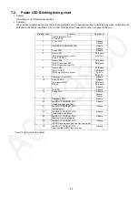
Page 23: ...ecovery circuit A SC FPC DET SC Board A SC FPC 7 Driver SOS2 SU SD Connector DET SU SD Scan and Logic IC SU Board SD Board 8 Driver SOS3 SS FPC DET SS Energy recovery circuit SS Board SS2 Board SS FPC SS2 FPC 9 Discharge Control SOS A Board 10 Sub 3 3V SOS Tuner power SOS BE SOS A Board SC Board SS Board P Board 11 Fan SOS A Board 12 Sound SOS A Board Speaker Woofer 13 Emergency SOS A Board 20 2nd...

Page 24: ... Power First check point There are following 3 states of No Power indication by power LED 1 No lit 2 Green is lit then turns red blinking a few seconds later See Power LED Blinking timing chart 3 Only red is lit ...

Page 25: ...25 7 4 No Picture ...

Page 26: ...26 7 5 Local screen failure Plasma display may have local area failure on the screen Fig 1 is the possible defect P C B for each local area Fig 1 ...

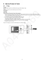
Page 27: ... be damaged if all connector is not removed for example remove connector only for SU board and stay connecting with SD board The board will be damaged 2 Connect SC jig to connector SC50 at left bottom side of SC board 3 Turn on the TV Display Unit and confirm the power LED blinking LED blinking Possible cause of failure is in SC board No LED blinking Lighting or no lighting Possible cause of failu...

Page 28: ...28 9 Disassembly and Assembly Instructions 9 1 Disassembly Flow Chart for the Unit This is a disassembly chart When assembling perform this chart conversely ...

Page 29: ...o the downside and remove the Pedestal stand 9 2 2 Remove the Stand bracket cover 1 Remove the screws 4 and remove the Stand bracket cover 9 2 3 Remove the AC cord clamper B 1 Remove the screws 2 and remove the AC cord clamper B 9 2 4 Remove the Wi LAN module 1 Remove the screw 1 and remove the Wi LAN module 9 2 5 Remove the Bluetooth module 1 Remove the screw 1 and remove the Bluetooth module 9 2...

Page 30: ...d the tapes to free the cables 2 Disconnect the connectors P2 P6 P9 P11 and P35 3 Remove the screws 6 and remove the P Board 9 2 9 Remove the A Board 1 Unlock the cable clampers and the tapes to free the cables 2 Disconnect the connectors A1 A6 A8 A12 and A50 3 Disconnect the USB cable JK8605 4 Disconnect the flexible cables A20 A31 A32 and A33 5 Remove the screws 3 6 Remove the Side shield metal ...

Page 31: ...pes to free the cables 2 Disconnect the Relay connector 3 Remove the screws 3 4 Remove the Woofer 9 2 13 Remove the Fan 1 Remove the screws 3 2 Remove the Relay connector and remove the Fan 9 2 14 Remove the SU Board 1 Disconnect the flexible cables SU1 SU2 SU3 SU4 and SU5 connected to the SU Board 2 Disconnect the flexible cable SU11 SD11 and the bridge connector SC41 SU41 3 Remove the screws 2 2...

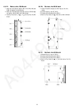
Page 32: ... screws 2 2 and remove the SD Board 9 2 16 Remove the SC Board 1 Unlock the cable clampers and the tapes to free the cables 2 Disconnect the connector SC2 3 Disconnect the flexible cable SC20 4 Remove the screws 8 and remove the SC Board 9 2 17 Remove the SS Board 1 Disconnect the connector SS11 2 Disconnect the flexible cable SS33 3 Disconnect the flexible cable SS52 4 Remove the screws 4 2 and r...

Page 33: ...per 2 Remove the USB cable from the USB clamper 9 2 20 Remove the BT connector clamper 1 Unlock the cable clampers and the tapes to free the cables 2 Remove the claws 2 and remove the BT cable 3 Disconnect the connector K1 and remove the A1 K1 cable 4 Remove the claws 2 and remove the BT connector clamper 9 2 21 Remove the Stand bracket plate 1 Remove the screws 4 2 2 and remove the Stand bracket ...

Page 34: ...uch as a table covered by a soft cloth with the Plasma panel surface facing downward 2 Remove the screws 10 3 Remove the Plasma panel section from the Cabinet assy 9 2 25 Remove the Contact metals 1 Remove the Tape from the Contact metals 2 Remove the screws 6 3 Remove the Contact metal side L R 4 Remove the screws 15 5 Remove the Contact metal bottom A 9 2 26 Remove the C1 Board 1 Disconnect the ...

Page 35: ... 9 2 29 Replace the Plasma panel Caution Remove the Plasma panel section from the servicing stand and lay on a flat surface such as a table covered by a soft cloth with the Plasma panel surface facing downward A new Plasma panel itself without Contact metals is fragile To avoid the damage to new Plasma panel carry a new Plasma panel taking hold of the Contact metals 1 Place a carton box packed a n...

Page 36: ...ess 5 button to display the On Screen Display 3 Press VOL button to set to LOW 4 In LOW setting a If no several dead pixel is visible remarkably in white pattern press 3 button to go to CONF stage b If the several dead pixels are visible remarkably in white pattern Set to HIGH by press VOL button Press 3 button to go to CONF stage if the symptom is improved 5 Press OK button in CONF stage to store...

Page 37: ...a ex D0 9 Set the color analyzer and adjust color point to the values written in table1 by using B DRIVE and R DRIVE 10 Increase RGB DRIVE value so that the maximum drive value of one of R DRIVE or G DRIVE or B DRIVE should become FF ALL DRIVE set to FF 11 Set the METHOD to 01 3 point adjustment 12 Check that the colour balance and the viewing mode is the values written in table1 and 2 13 INNER PA...

Page 38: ...38 ...

Page 39: ...ROCESSING VDDSD 18V33V SUB1 5V DCDC K P 3 3V SUB1 1V STB1 1V DCDC V YPbPr RGB P 1 2V ARC_OUT SUB3 3V DCDC C A T S SENSOR AUDIO SD CARD I F SOS6_SC1 LAN CON I F PEAKS PRO4 STB5V DCDC F15V PANEL_SOS TUNER_POWER_SOS SPI FLASH TMDS DATA AMP PEAKS EEPROM LVDS DATA P 15V DCDC SOS7_SC2 A6 HDMI I F P 15V PANEL_SOS P 15V_DET EV5V REMOTE_IN R DIGITAL AUDIO OUT DCDC15V L IEC_OUT SOUND_SOS K1 REMOTE RECEIVER ...

Page 40: ...UNER_SUB_ON PB PEAKS PRO4 DMD_ IIC0 AV IN 9 1 DDR3 I F DMD_ IIC1 SW_OFF_DET SOS4_PS HDMI_CEC DMD_ IIC1 IC8902 13 13 SD CARD I F STB1 1V C A T S AV SW 3 3V D1_R 5V DDC_IIC1 6 SUB5V HDMI_5V_DET2 USB3VBUS HDMI_CEC 2 PANEL_MAIN_ON HDMI_CEC 2 DRVRST A50 STB3 3V JK8601 1 5 3 3V BLUETOOTH HDMI3 3V SUB3 3V ARC DP1 SOUND_SOS IC8704 IC8705 D1_PR DM1 L_OUT SUB1 5V 10 3 VBUS1 DDC_IIC0 6 1 F15V L D1_PB 5V PD6H...

Page 41: ...C8702 SD_VCC 2 STB 1 1V SUB_AI3 3V REMOTE RECEIVER P 3 3V STB 3 3V R_LED_ON SUSTAIN CONTROL XRSTSTM DISPEN VIDEO DATA INIT_DONE IC9402 INIT_DONE 9 DISPEN SUSTAIN DATA BUFFER 1 1 LOGO_ON D_UHZ 2 5V FFC_OFF_DET SW_OFF_DET 6 LOGO_ON FFC_OFF_DET REMOTE RECEIVER 3 30 SPI FLASH 13 XRST 1 2V FAN_CHANGE DTV_RST C21 SI SO 1 IC9304 SCAN DATA BUFFER POWER_DET 12 SUB9V A8 KEYSCAN C A T S SENSOR 54 20MHz UHZ S...

Page 42: ...CUIT TRANSFOMER FOR RESONANCE Vda CONVERTER SWITCHING 140kHz typ Vda Vsus PHOTO COUPLER SWITCHING 90kHz 240kHz RESONANCE PFC OVP Vsus ERROR DET S0_S1 CIRCUIT PHOTO COUPLER PHOTO COUPLER TRANSFOMER FOR STANDBY STANDBY CONVERTER SWITCHING 65kHz typ Vcc AC_DET F_STBY ERROR DET PHOTO COUPLER RELAY RELAY P15V_ ON OFF F15V_ ON OFF P15V SWITCH F15V SWITCH 15Vc 15Vc OVP Vsus_ ON OFF PFC_ ON OFF STB5V CONV...

Page 43: ...NTROL 22 Q16600 SCAN CONTROL IC16921 VSCN F CELR NCRC1 SHUNT REG CEL IC16725 INVERTER NCRC1 SIU NCRC2 Q16451 CML 1 NCEL PANEL SUSTAIN ELECTRODE CIS NCVSET2 UML P 5V SUSTAIN DRIVE 30 IC16561 SUSTAIN CONTROL 25 VAD UML IPD CIRCUIT IC16786 87 P 15V SC2 CSH PC16301 SHUNT REG VSCN GEN VE GEN SS D16714 Q16051 RECOVERY L PC16897 USL IC16152 SHUNT REG Q16660 SS 11 UHZ VAD RECOVERY USH Vsus IC16151 SS 33 C...

Page 44: ...44 ...

Page 45: ...Diagram 12 1 Caution statement Caution Please confirm that all flexible cables are assembled correctly Also make sure that they are locked in the connectors Verify by giving the flexible cables a very slight pull 12 2 Wiring 1 ...

Page 46: ...46 12 3 Wiring 2 12 4 Wiring 3 ...

Page 47: ...Model No TX P50VT50B Y PR50VT50 Schematic Diagram Note S 1 ...

Page 48: ...Model No TX P50VT50B Y PR50VT50 Replacement Parts List Note S 2 ...

Page 49: ...Model No TX P50VT50B Y PR50VT50 A Board 1 14 S 3 ...

Page 50: ...Model No TX P50VT50B Y PR50VT50 A Board 2 14 S 4 ...

Page 51: ...Model No TX P50VT50B Y PR50VT50 A Board 3 14 S 5 ...

Page 52: ...Model No TX P50VT50B Y PR50VT50 A Board 4 14 S 6 ...

Page 53: ...Model No TX P50VT50B Y PR50VT50 A Board 5 14 S 7 ...

Page 54: ...Model No TX P50VT50B Y PR50VT50 A Board 6 14 S 8 ...

Page 55: ...Model No TX P50VT50B Y PR50VT50 A Board 7 14 S 9 ...

Page 56: ...Model No TX P50VT50B Y PR50VT50 A Board 8 14 and K Board S 10 ...

Page 57: ...Model No TX P50VT50B Y PR50VT50 A Board 9 14 S 11 ...

Page 58: ...Model No TX P50VT50B Y PR50VT50 A Board 10 14 S 12 ...

Page 59: ...Model No TX P50VT50B Y PR50VT50 A Board 11 14 S 13 ...

Page 60: ...Model No TX P50VT50B Y PR50VT50 A Board 12 14 S 14 ...

Page 61: ...Model No TX P50VT50B Y PR50VT50 A Board 13 14 S 15 ...

Page 62: ...Model No TX P50VT50B Y PR50VT50 A Board 14 14 S 16 ...

Page 63: ...Model No TX P50VT50B Y PR50VT50 C1 Board 1 2 S 17 ...

Page 64: ...Model No TX P50VT50B Y PR50VT50 C1 Board 2 2 S 18 ...

Page 65: ...Model No TX P50VT50B Y PR50VT50 C2 Board S 19 ...

Page 66: ...Model No TX P50VT50B Y PR50VT50 C3 Board S 20 ...

Page 67: ...Model No TX P50VT50B Y PR50VT50 SC Board 1 3 S 21 ...

Page 68: ...Model No TX P50VT50B Y PR50VT50 SC Board 2 3 S 22 ...

Page 69: ...Model No TX P50VT50B Y PR50VT50 SC Board 3 3 S 23 ...

Page 70: ...Model No TX P50VT50B Y PR50VT50 SS Board 1 2 S 24 ...

Page 71: ...Model No TX P50VT50B Y PR50VT50 SS Board 2 2 and SS2 Board S 25 ...

Page 72: ...Model No TX P50VT50B Y PR50VT50 A Board Foil side S 26 ...

Page 73: ...Model No TX P50VT50B Y PR50VT50 A Board Component side S 27 ...

Page 74: ...Model No TX P50VT50B Y PR50VT50 K Board S 28 ...

Page 75: ...Model No TX P50VT50B Y PR50VT50 C1 Board S 29 ...

Page 76: ...Model No TX P50VT50B Y PR50VT50 C2 Board S 30 ...

Page 77: ...Model No TX P50VT50B Y PR50VT50 C3 Board S 31 ...

Page 78: ...Model No TX P50VT50B Y PR50VT50 SC Board Foil side S 32 ...

Page 79: ...Model No TX P50VT50B Y PR50VT50 SC Board Component side S 33 ...

Page 80: ...Model No TX P50VT50B Y PR50VT50 SS Board Foil side S 34 ...

Page 81: ...Model No TX P50VT50B Y PR50VT50 SS Board Component side S 35 ...

Page 82: ...Model No TX P50VT50B Y PR50VT50 SS2 Board S 36 ...

Page 83: ...V 1 PAVCCZ C2000 F1G1E1030005 C 0 01UF 25V 1 C2001 F1J1A106A110 C 10UF 10V 1 PAVCCZ C2002 F1J1E105A287 C 1UF 25V 1 PAVCCZ C2003 F1J1E105A287 C 1UF 25V 1 PAVCCZ C2006 F1G1C104A077 C 0 1UF 16V 1 C2007 F1G1A105A047 C 1UF 10V 1 C2008 F1G1A105A047 C 1UF 10V 1 C2009 F1G1E1030005 C 0 01UF 25V 1 C2010 F1G1A105A047 C 1UF 10V 1 C2013 F1G1E1030005 C 0 01UF 25V 1 C2014 F1G1E1030005 C 0 01UF 25V 1 C2018 F1G1H1...

Page 84: ...F1J1A106A110 C 10UF 10V 1 PAVCCZ C3187 F1J1A106A110 C 10UF 10V 1 PAVCCZ C3202 F1G1C104A077 C 0 1UF 16V 1 C3304 F2H1A101A040 C 100UF 10V 1 C3306 F2H1A101A040 C 100UF 10V 1 C3851 F1G1A105A047 C 1UF 10V 1 C3852 F1G1C104A077 C 0 1UF 16V 1 C3853 F1G1C104A077 C 0 1UF 16V 1 C3854 F1G1C104A077 C 0 1UF 16V 1 C3855 F1G1C104A077 C 0 1UF 16V 1 C4551 F1G1A105A047 C 1UF 10V 1 C4900 F1K1V106A010 C 10UF 25V 1 PAV...

Page 85: ...1G1C104A077 C 0 1UF 16V 1 C6711 F1J1A106A110 C 10UF 10V 1 PAVCCZ C6718 F1G1H101A834 C 100PF 50V 1 PAVCCZ C6719 F1G1H220A834 C 22PF 50V 1 PAVCCZ C6720 F1G1H220A834 C 22PF 50V 1 PAVCCZ C6721 F1G1H220A834 C 22PF 50V 1 PAVCCZ C6722 F1G1E472A144 C 4700pF 25V 1 PAVCCZ C6723 F1G1H101A834 C 100PF 50V 1 PAVCCZ C6724 F1G1H101A834 C 100PF 50V 1 PAVCCZ C6725 F1G1H220A834 C 22PF 50V 1 PAVCCZ C6726 F1G1H220A834...

Page 86: ... C 1 uF 16 V 1 C8112 F1G1C104A077 C 0 1UF 16V 1 C8113 F1K1E106A134 C 10UF 25V 1 C8115 F1J0G2260001 C 22 UF 4 V 1 C8116 F1J0G2260001 C 22 UF 4 V 1 C8118 ECJ1VB1E104K C 0 1 UF 25V 1 C8120 F1G1E682A059 C 6800PF 25V 1 PAVCCZ C8121 F1H1C105A145 C 1 uF 16 V 1 C8122 F1J1A475A112 C 4 7UF 10V 1 PAVCCZ C8123 F1G1C104A077 C 0 1UF 16V 1 C8124 F1K1E106A134 C 10UF 25V 1 C8125 F1K1E106A134 C 10UF 25V 1 C8126 F1J...

Page 87: ...A049 C 22UF 6 3V 1 C8403 F1K0J226A049 C 22UF 6 3V 1 C8406 F1G1C104A077 C 0 1UF 16V 1 C8407 F1G1C104A077 C 0 1UF 16V 1 C8600 F1H1C105A145 C 1 uF 16 V 1 C8602 F1G1H120A834 C 12PF 50V 1 PAVCCZ C8603 F1G1H120A834 C 12PF 50V 1 PAVCCZ C8604 F1G1C104A077 C 0 1UF 16V 1 C8605 F1G1C104A077 C 0 1UF 16V 1 C8607 F1G1C104A077 C 0 1UF 16V 1 C8608 F1G1C104A077 C 0 1UF 16V 1 C8609 F1H1C105A145 C 1 uF 16 V 1 C8610 ...

Page 88: ... 25V 1 C8724 F1J1A106A110 C 10UF 10V 1 PAVCCZ C8725 F1J1A106A110 C 10UF 10V 1 PAVCCZ C8728 F1H1C105A145 C 1 uF 16 V 1 C8729 F1G1E472A086 C 4700pF 25V 1 C8730 F1G1C104A077 C 0 1UF 16V 1 C8731 F1G1E1030005 C 0 01UF 25V 1 C8732 F1K1V106A010 C 10UF 25V 1 PAVCCZ C8733 F1J1A106A110 C 10UF 10V 1 PAVCCZ C8734 F1J1A106A110 C 10UF 10V 1 PAVCCZ C8737 F1G1C104A077 C 0 1UF 16V 1 C8738 F1G1H222A830 C 2200PF 50V...

Page 89: ... 1 C9347 F1G1A105A047 C 1UF 10V 1 C9354 F1G1A105A047 C 1UF 10V 1 C9355 F1J1A106A110 C 10UF 10V 1 PAVCCZ C9356 F1J1A106A110 C 10UF 10V 1 PAVCCZ C9357 F1J1A106A110 C 10UF 10V 1 PAVCCZ C9366 F1G1A105A047 C 1UF 10V 1 C9367 F1G1A105A047 C 1UF 10V 1 C9368 F1G1A105A047 C 1UF 10V 1 C9371 F1J1A106A110 C 10UF 10V 1 PAVCCZ C9375 F1G1C104A077 C 0 1UF 16V 1 C9376 F1G1A105A047 C 1UF 10V 1 C9378 F1G1C104A077 C 0...

Page 90: ...ER 1 PAVCCZ D3002 J0ZZB0000175 FILTER 1 PAVCCZ D3003 DZ2J140M0L ZENER DIODE 1 D3004 DZ2J140M0L ZENER DIODE 1 D3100 J0ZZB0000175 FILTER 1 PAVCCZ D3101 J0ZZB0000175 FILTER 1 PAVCCZ D3102 J0ZZB0000175 FILTER 1 PAVCCZ D3130 B0JCCE000021 DIODE 1 D3201 K7AAAY000014 PHOTO LINK 1 PAVCCZ D4703 DZ2J056M0L ZENER DIODE 1 D4720 DZ2J056M0L ZENER DIODE 1 D4771 DZ2J056M0L ZENER DIODE 1 D4773 B0JCCE000021 DIODE 1 ...

Page 91: ...AVCCZ IC8902 X24CP50VT50Y IC 1 Y PAVCCZ IC8902 X24CPR50VT50 IC 1 PR PAVCCZ IC9005 C0CBCAG00046 IC 1 IC9300 C1AB00003813 IC 1 PAVCCZ IC9304 TVRS677AC IC 1 PAVCCZ IC9400 C0JBAZ001120 IC 1 IC9401 C0JBAZ001120 IC 1 IC9402 C0JBAZ001120 IC 1 IC9803 C0DBAYY01283 IC 1 PAVCCZ IC9804 C0DBZYY00541 IC 1 PAVCCZ JK3002 K1FY120E0002 CONNECTOR 1 PAVCCZ JK3100 K2HE2YYB0001 JACK 1 PAVCCZ JK3103 K2HC1YYB0077 JACK 1 ...

Page 92: ...2 J0JYC0000464 FILTER 1 PAVCCZ L8013 J0JYC0000464 FILTER 1 PAVCCZ L8101 G1C4R7ZA0311 INDUCTION COIL 1 PAVCCZ L8102 G1C1R0MA0535 INDUCTION COIL 1 PAVCCZ L8600 J0ZZB0000142 FILTER 1 L8601 J0ZZB0000142 FILTER 1 L8602 J0ZZB0000142 FILTER 1 L8603 J0ZZB0000142 FILTER 1 L8604 J0JYC0000464 FILTER 1 PAVCCZ L8605 J0JYC0000464 FILTER 1 PAVCCZ L8606 J0JYC0000464 FILTER 1 PAVCCZ L8607 J0JYC0000464 FILTER 1 PAV...

Page 93: ...GA272JA023 M 2 7KOHM J 1 16W 1 R0910 D0GA272JA023 M 2 7KOHM J 1 16W 1 R0911 D1HY3324A012 NETWORK RESISTER 1 PAVCCZ R0912 D0GA101JA023 M 100 OHM J 1 16W 1 R0913 D0GA101JA023 M 100 OHM J 1 16W 1 R0922 D1HY3324A012 NETWORK RESISTER 1 PAVCCZ R0936 D0GA360JA023 M 36 OHM J 1 16W 1 R0937 D0GA360JA023 M 36 OHM J 1 16W 1 R0941 D0GA360JA023 M 36 OHM J 1 16W 1 R0942 D0GA360JA023 M 36 OHM J 1 16W 1 R0943 D0GA...

Page 94: ... J 1 16 W 1 R2016 D0GA104JA023 M100KOHM J 1 16 W 1 R2017 D0GA102JA023 M1KOHM J 1 16 W 1 R2018 D0GA102JA023 M1KOHM J 1 16 W 1 R2023 D0GA472JA023 M 4 7KOHM J 1 16W 1 R2024 D0GA223JA023 M 22K OHM J 1 16W 1 R2025 D0GA103JA023 M10KOHM J 1 16 W 1 R2033 D0GA103JA023 M10KOHM J 1 16 W 1 R2035 D0GA223JA023 M 22K OHM J 1 16W 1 R2036 D0GA223JA023 M 22K OHM J 1 16W 1 R2038 D0GA162JA023 M 1 6KOHM J 1 16W 1 PAVC...

Page 95: ... R3204 D1BA2152A023 M 21 5KOHM F 1 16 W 1 PAVCCZ R3206 D1BA1302A023 M 13KOHM F 1 16W 1 PAVCCZ R3208 D0GA273JA023 M 27K OHM J 1 16W 1 R3211 D0GA360JA023 M 36 OHM J 1 16W 1 R3212 D0GBR00J0004 M 0 OHM J 1 10W 1 R3220 D0GA104JA023 M100KOHM J 1 16 W 1 R3221 D1HY6804A012 NETWORK RESISTER 1 PAVCCZ R3222 D0GA514JA023 M 510KOHM J 1 16W 1 PAVCCZ R3230 D0GA101JA023 M 100 OHM J 1 16W 1 R3290 D0GA473JA023 M 47...

Page 96: ...8 D0GA273JA023 M 27K OHM J 1 16W 1 R4900 D0GFR00J0005 M 0 OHM J 1 3W 1 R4901 D1HY6804A012 NETWORK RESISTER 1 PAVCCZ R4902 D0GA680JA023 M 68 OHM J 1 16W 1 R4906 D0GA472JA023 M 4 7KOHM J 1 16W 1 R4907 D0GA102JA023 M1KOHM J 1 16 W 1 R4908 D0GA102JA023 M1KOHM J 1 16 W 1 R4917 D0GA472JA023 M 4 7KOHM J 1 16W 1 R4918 D0GA472JA023 M 4 7KOHM J 1 16W 1 R4958 D0GA103JA023 M10KOHM J 1 16 W 1 R4959 D0GA103JA02...

Page 97: ...0 OHM F 1 16 W 1 PAVCCZ R8217 D0GA221JA023 M220 OHM J 1 16 W 1 R8218 D0GA221JA023 M220 OHM J 1 16 W 1 R8219 D1BA2400A023 M 240 OHM F 1 16 W 1 PAVCCZ R8220 D1BA2400A023 M 240 OHM F 1 16 W 1 PAVCCZ R8221 D0GA103JA023 M10KOHM J 1 16 W 1 R8230 D1BA2700A023 M 270 OHM F 1 16 W 1 PAVCCZ R8231 D1BA2700A023 M 270 OHM F 1 16 W 1 PAVCCZ R8232 D1BA2700A023 M 270 OHM F 1 16 W 1 PAVCCZ R8233 D1BA2700A023 M 270 ...

Page 98: ...3JA023 M 22K OHM J 1 16W 1 R8441 D0GA103JA023 M10KOHM J 1 16 W 1 R8444 D0GA103JA023 M10KOHM J 1 16 W 1 R8445 D1HY6804A012 NETWORK RESISTER 1 PAVCCZ R8446 D1HY6804A012 NETWORK RESISTER 1 PAVCCZ R8447 D0GA103JA023 M10KOHM J 1 16 W 1 R8509 D0GA103JA023 M10KOHM J 1 16 W 1 R8601 D1BA75R0A023 M 75 0 OHM F 1 16 W 1 PAVCCZ R8602 D1BA75R0A023 M 75 0 OHM F 1 16 W 1 PAVCCZ R8603 D1BA75R0A023 M 75 0 OHM F 1 1...

Page 99: ... D0GBR00J0004 M 0 OHM J 1 10W 1 R8694 D1BA3742A023 M 37 4 KOHM F 1 16 W 1 PAVCCZ R8695 D1BA1822A023 M 18 2KOHM F 1 16 W 1 PAVCCZ R8696 D1BA3742A023 M 37 4 KOHM F 1 16 W 1 PAVCCZ R8699 D0GA103JA023 M10KOHM J 1 16 W 1 R8707 D0GBR00J0004 M 0 OHM J 1 10W 1 R8711 D0GA473JA023 M 47KOHM J 1 16W 1 R8712 D0GA102JA023 M1KOHM J 1 16 W 1 R8713 D0GA510JA023 M 51 OHM J 1 16W 1 PAVCCZ R8714 D1BA4702A023 M 47 KOH...

Page 100: ... 1 PAVCCZ R9118 D0GB123ZA038 M 12KOHM J 1 10W 1 PAVCCZ R9126 D0GA101JA023 M 100 OHM J 1 16W 1 R9127 D0GA101JA023 M 100 OHM J 1 16W 1 R9160 D0GA103JA023 M10KOHM J 1 16 W 1 R9163 D0GA103JA023 M10KOHM J 1 16 W 1 R9164 D0GA103JA023 M10KOHM J 1 16 W 1 R9165 D0GA472JA023 M 4 7KOHM J 1 16W 1 R9168 D0GA472JA023 M 4 7KOHM J 1 16W 1 R9198 D1HY6804A012 NETWORK RESISTER 1 PAVCCZ R9199 D0GA473JA023 M 47KOHM J ...

Page 101: ...TOR 1 PAVCCZ C11 K1MY55BA0345 55P CONNECTOR 1 C14 K1KY03AA0719 3P CONNECTOR 1 C20 K1KY03BA0387 3P CONNECTOR 1 PAVCCZ C21 K1MY55BA0345 55P CONNECTOR 1 C25 K1KY04BA0387 4P CONNECTOR 1 PAVCCZ C26 K1MY40BA0345 40P CONNECTOR 1 C36 K1MY40BA0345 40P CONNECTOR 1 C16003 F1L2J562A021 C 5600PF 630V 1 PAVCCZ C16011 F2A2E261A290 E 260UF 250V 1 PAVCCZ C16012 F2A2E261A290 E 260UF 250V 1 PAVCCZ C16013 F2A2E261A29...

Page 102: ...CCZ C16415 F0C2E105A307 C 1UF 250V 1 PAVCCZ C16423 F1L2J562A021 C 5600PF 630V 1 PAVCCZ C16441 ECJ1VB1H392K C 3900UF 50V 1 C16442 ECJ1VB1H392K C 3900UF 50V 1 C16450 F1L2J472A021 C 4700PF 630V 1 PAVCCZ C16451 ECJ1VB1H392K C 3900UF 50V 1 C16452 ECJ1VB1H392K C 3900UF 50V 1 C16460 F1K2J222A024 C 2200PF 630V 1 PAVCCZ C16502 F1K1E475A134 C 4 7UF 25V 1 C16503 F2A1E151B705 E 150UF 25V 1 C16505 F1K1E105A029...

Page 103: ...99 C 1UF 10V 1 PAVCCZ C17102 F1H1A105A099 C 1UF 10V 1 PAVCCZ C17103 F1H1A105A099 C 1UF 10V 1 PAVCCZ C17108 F1L2E224A028 C 0 22UF 250V 1 C17109 F1L2E224A028 C 0 22UF 250V 1 C17111 F1L2E224A028 C 0 22UF 250V 1 C17131 F1H1A105A099 C 1UF 10V 1 PAVCCZ C17132 F1H1A105A099 C 1UF 10V 1 PAVCCZ C17134 F1L2E224A028 C 0 22UF 250V 1 C17136 F1L2E224A028 C 0 22UF 250V 1 C17137 F1H1A105A099 C 1UF 10V 1 PAVCCZ C17...

Page 104: ...DE 1 PAVCCZ D16053 B0FCCN000005 DIODE 1 PAVCCZ D16071 B0ECKP000055 DIODE 1 D16072 B0ECKP000055 DIODE 1 D16131 B0ECKP000055 DIODE 1 D16133 DA2J10100L DIODE 1 D16134 DZ2J051M0L ZENER DIODE 1 D16135 DA2J10100L DIODE 1 D16191 B0ECKP000055 DIODE 1 D16192 DA2J10100L DIODE 1 D16196 DZ2J200M0L ZENER DIODE 1 D16243 DA3X103E0L DIODE 1 PAVCCZ D16251 DZ2J330M0L ZENER DIODE 1 D16252 DZ2J330M0L ZENER DIODE 1 D1...

Page 105: ...D16728 B0ECKP000055 DIODE 1 D16823 DA3X103E0L DIODE 1 PAVCCZ D16824 DA2J10100L DIODE 1 D16825 DZ2J330M0L ZENER DIODE 1 D16826 DZ2J330M0L ZENER DIODE 1 D16828 DA2J10100L DIODE 1 D16833 B0ECHR000004 DIODE 1 D17103 B0JCCD000020 DIODE 1 D17303 B0JCCD000020 DIODE 1 HS16001 K4AZ02D00004 TERMINAL 1 PAVCCZ HS16002 K4AZ02D00004 TERMINAL 1 PAVCCZ HS16003 K4AZ02D00004 TERMINAL 1 PAVCCZ HS16021 K4AZ02D00004 T...

Page 106: ...787 C0DBZYY00532 IC 1 PAVCCZ IC16795 C0CBALC00012 IC 1 IC16921 C1ZBZ0004557 IC 1 PAVCCZ IC17101 C0JBAU000088 IC 1 IC17201 C0JBAU000088 IC 1 IC17301 C0JBAU000088 IC 1 L16001 G0CR43ZA0053 PEAKING COIL 1 PAVCCZ L16002 G0CR43ZA0053 PEAKING COIL 1 PAVCCZ L16021 G0ZZ00002183 PEAKING COIL 1 L16022 G0ZZ00002183 PEAKING COIL 1 L16023 G0ZZ00002183 PEAKING COIL 1 L16024 G0ZZ00002183 PEAKING COIL 1 L16070 G0Z...

Page 107: ...6 TRANSISTOR 1 PAVCCZ Q16581 B1ABCF000231 TRANSISTOR 1 Q16600 B1CFRM000020 FET 1 Q16601 B1CFRQ000021 FET 1 Q16602 B1CFGF000019 FET 1 PAVCCZ Q16621 B1JBDN000004 TRANSISTOR 1 Q16622 B1JBDN000004 TRANSISTOR 1 Q16623 B1JBDN000004 TRANSISTOR 1 Q16624 B1JBDN000004 TRANSISTOR 1 Q16646 B1CFGF000019 FET 1 PAVCCZ Q16647 B1CBGD000001 FET 1 Q16648 DSC2001Q0L TRANSISTOR 1 Q16652 B1ADCE000027 TRANSISTOR 1 Q1666...

Page 108: ...2 2KOHM J 1 10W 1 R16283 D0GB473JA065 M 47KOHM J 1 10W 1 R16285 D0GB623JA065 M 62KOHM J 1 10W 1 PAVCCZ R16287 D0GF334JA047 M 330KOHMJ 1 3W 1 R16291 D0GB103JA065 M 10K OHM J 1 10W 1 R16307 D1BD5232A147 M 52 3KOHM F 1 8W 1 PAVCCZ R16309 D0GF273JA054 M 27 KOHM 1 2W 1 PAVCCZ R16311 D0GF273JA054 M 27 KOHM 1 2W 1 PAVCCZ R16317 D1BD5762A147 M 57 6KOHM F 1 8W 1 PAVCCZ R16318 D1BD5762A147 M 57 6KOHM F 1 8W...

Page 109: ...A048 M 56 KOHM J 1 3W 1 R16583 D1BD1003A066 M 100KOHM F 1 8 W 1 R16584 D1BD3742A066 M 37 4KOHM F 1 8W 1 PAVCCZ R16585 D0GB473JA065 M 47KOHM J 1 10W 1 R16587 D0GB222JA065 M 2 2KOHM J 1 10W 1 R16588 D0GB223JA065 M 22KOHM J 1 10W 1 R16590 D0GB221JA065 M 220 OHM J 1 10W 1 R16601 D0GF1R0JA047 M 1 OHM J 1 3W 1 R16602 D0GB220JA065 M 22 OHM J 1 10W 1 R16603 D0GF153JA047 M 15 KOHM J1 3W 1 PAVCCZ R16604 D0G...

Page 110: ...8 1KOHM F 1 8W 1 PAVCCZ R16832 D1BD7152A147 M 71 5KOHM F 1 8W 1 PAVCCZ R16833 D0GF683JA048 M 68 KOHM J 1 4W 1 PAVCCZ R16834 D0GF683JA048 M 68 KOHM J 1 4W 1 PAVCCZ R16835 D0GF683JA048 M 68 KOHM J 1 4W 1 PAVCCZ R16836 D0GF683JA048 M 68 KOHM J 1 4W 1 PAVCCZ R16839 ERG2FJX473 M 47KOHM J 1W 1 R16840 ERG2FJX473 M 47KOHM J 1W 1 R16841 D0GB472JA065 M 4 7KOHM J 1 10W 1 R16842 D0GD102JA052 M 1 0KOHM J 1 8W ...

Page 111: ...A047 M 1 OHM J 1 3W 1 R17126 D0GB101JA065 M 100 OHM J 1 10W 1 R17127 D0GB101JA065 M 100 OHM J 1 10W 1 R17128 D0GB101JA065 M 100 OHM J 1 10W 1 R17129 D0GB101JA065 M 100 OHM J 1 10W 1 R17130 D0GF1R0JA047 M 1 OHM J 1 3W 1 R17132 D0GF1R0JA047 M 1 OHM J 1 3W 1 R17134 D0GD224JA052 M 220KOHM J 1 8W 1 R17135 D0GB681JA065 M 680 OHM J 1 10W 1 R17138 D1H84704A041 NETWORK RESISTER 1 PAVCCZ R17139 D1H84704A041...

Page 112: ...CCZ R17352 D1H84704A041 NETWORK RESISTER 1 PAVCCZ R17353 D0GB470JA065 M 47 OHM J 1 10W 1 R17395 D0GD151JA059 M 150 OHM J 1 4W 1 R17396 D0GB331JA065 M330 OHM J 1 10W 1 SC2 K1KY02C00002 2P CONNECTOR 1 PAVCCZ SC20 K1MY30BA0345 30P CONNECTOR 1 SC41 K1KA09AA0707 9P CONNECTOR 1 SC42 K1KA09AA0707 9P CONNECTOR 1 SC46 K1KA09AA0707 9P CONNECTOR 1 SC50 K1KA02AA0193 2P CONNECTOR 1 SS11 K1KY02C00002 2P CONNECT...

Page 113: ...Model No TX P50VT50B Y PR50VT50 Exploded View 1 S 67 ...

Page 114: ...Model No TX P50VT50B Y PR50VT50 Exploded View 2 S 68 ...

Page 115: ...Model No TX P50VT50B Y PR50VT50 Packing 1 S 69 ...

Page 116: ...Model No TX P50VT50B Y PR50VT50 Packing 2 S 70 ...

Page 117: ...Model No TX P50VT50B Y PR50VT50 Packing 3 S 71 ...

Page 118: ...SH 8 24 chap 9 2 6 1 THEC164J SCREW WOOFER 3 3 PAVCCZ THEJ036J SCREW CON_A B 6 STD_BRA 2 K 1 9 THEJ036J SCREW P 6 SS 4 SC 8 SUSD 3 SS2 2 CONT L 7 R 3 33 THEJ036J SCREW C 10 DD CONTACT_BOT 15 25 THEJ039J SCREW 6 THEL0239 SCREW TU 2 AC_BRA 2 STD_BRA CONT_B 2 6 chap 9 2 6 2 11 TKK5ZC50231 LED PANEL 1 PAVCCZ 12 TKKL5493 M8 CAP 4 chap 9 2 6 3 13 TKP0EA00701 CI BRACKET 1 PAVCCZ 14 TKP0EA01201 STAND BRAC...

Page 119: ...CTION BOOK ENGLISH 1 Y PAVCCZ 73 TQB0E2252V INSTRUCTION BOOK CROATIAN 1 Y PAVCCZ 73 TQB0E2252W INSTRUCTION BOOK SLOVAKIAN 1 Y PAVCCZ 73 TQB0E2252Z INSTRUCTION BOOK ESTONIAN 1 Y PAVCCZ 73 TQB0E22549 INSTRUCTION BOOK KAZAKHSTAN 1 PR PAVCCZ 73 TQB0E2254L INSTRUCTION BOOK RUSSIAN 1 PR PAVCCZ 73 TQB0E2254Y INSTRUCTION BOOK UKRAINIAN 1 PR PAVCCZ 74 TQB0E2252X INSTRUCTION BOOK CD ROM 1 Y PAVCCZ 75 TQD0E1...

Reviews: