208
FEB 2008
Ver. 1.1
DP-C405/C305/C265
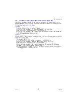
3.10. Power on Display Change (F9-19)
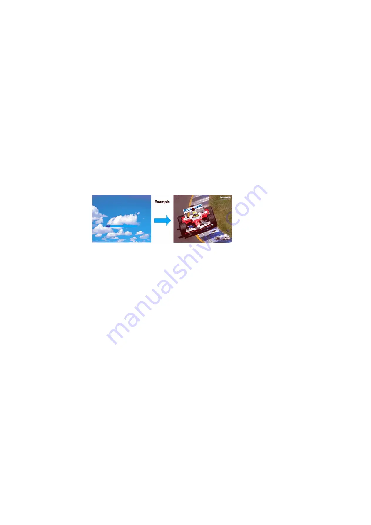
To change the startup Panel Display (when the Power Switch on the Left Side is turned ON) follow the
procedure below. This feature is useful if a Dealer wants to personalize the machine with its own company's
Logo or Picture (New feature for DP-C405 Series).
<Prepare>
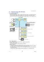
1. Save your selected JPEG image file onto the designated folder in the SD Memory Card using a
designated file name.
Designated Folder
: \private\meigroup\pcc\di\image\ (Default folder for Scan to SD Card)
Designated File
: image.jpg
(Default file name for Scan to SD Card)
Designated File type : JPEG
<Procedure>
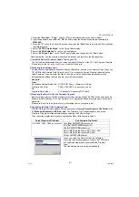
1. Install the SD Memory Card into the Front SD Card Slot.
2. Select the Service Parameter
“F9-19 Power On Display”
, then select
“Custom”
and
“OK”
.
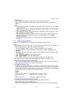
3. Select
“OK”
to register the image.
Note:
1. Use an appropriate sized (640 x 480 pixels) image data to fit into the Display Panel without cropping or
cutting off.
Example:
If the image size is A4 the display will have borders filled in Light Blue.
2. The image file for Custom setting is saved in the F-ROM on the SC PCB.
3. When the SC firmware is updated or RAM Initialize (Shipment Set, Parameter Initialize) is executed,
the Custom image file is deleted, and the display returns to the Original default screen setting.
Summary of Contents for Workio DP-C305
Page 2: ...2...
Page 3: ...3...
Page 5: ...5...
Page 6: ...6 For PB and Other Destinations not for PU USA Canada...
Page 11: ...11...
Page 12: ...12...
Page 13: ...13...
Page 14: ...14 memo...
Page 220: ...220 FEB 2008 Ver 1 1 DP C405 C305 C265 Color Test Chart 101 P N PJQRC0119Z LDR PJQRC0120Z A3...
Page 232: ...232 FEB 2008 Ver 1 1 DP C405 C305 C265 3 20 720K PM Kit DQ M35S72 DQ M32N72...
Page 400: ...400 FEB 2008 Ver 1 1 DP C405 C305 C265 LVPS CN6 LVPS CN7 Refer to SCN PC Board...
Page 401: ...401 FEB 2008 Ver 1 1 DP C405 C305 C265 LVPS CN8 Europe Specification Only...
Page 404: ...404 FEB 2008 Ver 1 1 DP C405 C305 C265 CST PCB CN603 CST PCB CN604...
Page 405: ...405 FEB 2008 Ver 1 1 DP C405 C305 C265 CST PCB CN605...
Page 406: ...406 FEB 2008 Ver 1 1 DP C405 C305 C265...
Page 407: ...407 FEB 2008 Ver 1 1 DP C405 C305 C265 CST PCB CN606...
Page 408: ...408 FEB 2008 Ver 1 1 DP C405 C305 C265...
Page 409: ...409 FEB 2008 Ver 1 1 DP C405 C305 C265 CST PCB CN607...
Page 410: ...410 FEB 2008 Ver 1 1 DP C405 C305 C265 CST PCB CN608...
Page 412: ...412 FEB 2008 Ver 1 1 DP C405 C305 C265 TRU PCB CN613...
Page 414: ...414 FEB 2008 Ver 1 1 DP C405 C305 C265 RLB PCB CN176...
Page 615: ...615 DP C405 C305 C265 FEB 2008 Ver 1 1 1 2 3 4 5 6 7 8...
Page 752: ...752 FEB 2008 Ver 1 1 DP C405 C305 C265 memo...
Page 847: ...847 DP C405 C305 C265 FEB 2008 Ver 1 1 2 Motor PCBs Fig 5 009 M1 M2 M8 M5 M4 M3 M7 M6 1...
Page 919: ......
Page 920: ...Published in Japan...


