background image

3DQDVRQLF

10

1.1.4  Horizontal and vertical synchronization

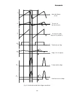
See also the related block diagram as well as the diagrams at the end of the report.
The main functions are:
* Horizontal sync separator
* Horizontal oscillator and calibration system
* PHI-1 detector
* PHI-2 detector and sandcastle generation
* Horizontal output with slow start/stop facility
* Coincidence detector
* Noise detector
* Vertical sync separator
* Vertical divider system

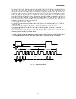
* Horizontal sync separator
The horizontal sync separator is supplied from the CVBS/Y inputs (chosen video source). For
horizontal synchronization the sync separator slices in the middle of the sync pulse and the slicing
level is independent of the sync pulse amplitude. For the vertical synchronization the sync pulse is
sliced at a level of about 30% (closer to the black level). This ensures optimal output signals for a
stable horizontal and vertical deflection under various video input conditions.
The top sync level is clamped at the CVBS input. The black level is stored internally.

* Horizontal oscillator and calibration system
The horizontal oscillator requires no external components and is fully integrated. The adjustment for
nominal frequency is derived automatically by a calibration circuit.
The oscillator generates a sawtooth signal with double horizontal frequency. This sawtooth signal is
used to derive several other gating and timing signals. After calibration the horizontal oscillator is
controlled by the PHI-1 loop for synchronization with the incoming video input signal.
The calibrator is responsible for the automatic adjustment of the horizontal oscillator. One of the color
crystals is being used as reference. For that reason a correct crystal selection by XA,XB (Xtal
selection) is very important during power-on. Calibration occurs during the vertical retrace period and
only under following conditions:
- At power-on/ initialization
- After power dip (shutdown detection), re-initialization is required.
- After loss of synchronization (e.g. after channel switching)

* PHI-1 detector
The PHI-1 detector is a PLL circuit that synchronizes the horizontal oscillator with the incoming video
signal. The PLL compares the output of the H-sync separator with the horizontal oscillator. The PLL
output current is converted to a voltage by means of the external loop filter. This voltage controls the
horizontal oscillator. The loop filter is connected externally so the time constant can be defined
according to the customer requirements. Because the static loop gain is very high there will be no
phase shift when switching between input signals with different line.

* PHI-2 detector and sandcastle
As described, the Horizontal PLL (PHI-1 loop) synchronizes the horizontal oscillator with the incoming
video signal. The PHI-2 loop provides a stable picture position on screen.
This is necessary because due to beam current variations the storage time of the line transistor varies
and, due to that, the picture position on screen.
The PHI-2 detector compares the horizontal oscillator signal (reference) with the horizontal flyback
input pulse, pin 41. This flyback pulse is related to the horizontal deflection.
The PHI-2 circuit shifts the horizontal drive, pin 40, such that the picture position on screen is constant.
The flyback input pin 41 is combined with the sandcastle output. This combined function provides a
three level sandcastle signal and is available starting with the highest level: burstkey, line blanking (=
flyback pulse) and vertical blanking.

The phase of the video signal with respect to the deflection current can be adapted by I²C bus HS
(horizontal shift, shift picture left/right).
The PHI-2 loop filter is a first order filter. The capacitor is connected externally on pin 42.

Summary of Contents for Z-421V

Page 1: ...Technical Guide Colour Television Z 421V Chassis Circuit Description Panasonic European Television Division Matsushita Electric U K Ltd Order No TG 990904 ...

Page 2: ... 2 Drive circuit part 30 1 5 VIDEO AMPLIFIER AND ABS 32 1 5 1 Video output amplification 32 1 5 2 ABS operation 34 1 5 3 Beam current limiter 35 1 5 4 Euro scart 36 1 6 POWER SUPPLY STR S5707 37 1 6 1 Vin terminal start up circuit 37 1 6 2 Oscillator F B terminal voltage pin 7 37 1 6 3 Function of INH terminal pin 6 control of off time 37 1 6 4 Drive circuit 37 1 6 5 OCP function 37 1 6 6 Latch Ci...

Page 3: ...e of mechanical surface waves TV standard B G L L I Picture carrier 38 9 MHz 38 9 MHz 38 9 MHz Color carrier 34 47 MHz 34 47 MHz 34 47 MHz Sound carrier 33 4 MHz 33 4 MHz 33 4 MHz 1 1 2 Vision IF See also the related block diagram as well as the diagrams at the end of the report The main functions are IF amplifier PLL demodulator and alignment free VCO Video buffer AFC AGC Tuner AGC Video identifi...

Page 4: ... occurs automatically after power on and every time after loss of sync lock I 2 C bit SL The PLL catching range is plus min 1MHz around the selected IF frequency Within this range the PLL ensures automatic tracking to the incoming frequency The PLL is basically an FPLL Frequency Phase Lock Loop system This extra frequency detector gives an output signal to the PLL loopfilter as long as a differenc...

Page 5: ...tive modulation For positive modulated signals the AGC is a top white AGC including black level clamp which making the video amplitude independent of video contents A top white AGC requires a 100 white reference pulse in order to be independent of video contents Suitable for that purpose is the white pulse Video Insertion Test Signal VITS in line 17 and 330 see Fig 2 Because the time constant is l...

Page 6: ... below 80 white level If the speed up is activated the AGC capacitor will be discharged with a current of 50mA Tuner AGC The tuner AGC is provided to reduce the tuner gain and thus the tuner output voltage when receiving strong RF signals The tuner AGC takes over when the IF input reaches a certain input level that can be adjusted by I C function AGC take over The tuner gain can be reduced by mean...

Page 7: ...ating AGC detector LPF LPF Demodulator Calibrator AFC IFA IFB IFC IF frequency selection AFW AFA AFB f sc MOD pos Neg VSW Video mute Video Ident IF1 PLL loopfilter AGC decoupling N C IF input 1 IF input 2 Tuner AGC out IF Video out 4 3 48 49 54 53 6 5 Fig 4 Block diagram Vision IF ...

Page 8: ...umption The PLL catching range is 4 2 6 8MHz which is suitable for all multistandard applications Pre amplifier and mute The pre amplifier output signal available at the deemphasis pin can be used for SCART application At this pin the deemphasis capacitor has to be connected The output level is 500mVrms for a FM swing of 50kHz A pre amplifier with DC feedback has been provided The DC component of ...

Page 9: ...me FAV Fixed audio INA INB INC MOD XA 0 0dB XA 1 6dB VCO Automatic volume level Volume control 1 10MHz 15k 3V 15dB 71dB 500mVrms max 2Vrms 500mVrms 50kHz swep 250mVrms 25kHz sweep AVL feature not on all models Sound mute INT mode via SL 0 SM 1 EXT mode via IFl 0 SM 1 STB 0 SM 1 No mute VIM 1 Sound IF in Deemphasis Audio line out Audio out Fig 5 Block diagram Sound ...

Page 10: ...power on Calibration occurs during the vertical retrace period and only under following conditions At power on initialization After power dip shutdown detection re initialization is required After loss of synchronization e g after channel switching PHI 1 detector The PHI 1 detector is a PLL circuit that synchronizes the horizontal oscillator with the incoming video signal The PLL compares the outp...

Page 11: ...oincidence detector can be made less sensitive about 5 dB by control bit STM search tuning mode This prevents false stops Vertical sync separator The vertical sync separator separates the vertical sync pulse from the composite sync signal This separated sync pulse is used to trigger the vertical divider system To generate a trigger pulse for the divider the minimum pulse width of the incoming vert...

Page 12: ...annel switching the system can be forced to the search window by means of I C bus setting NCIN 1 vertical divider mode Immediate after forcing to search mode NCIN has to be set back to 0 for optimum performance The vertical synchronization mode of operation can be selected by I C bus FORF S forced field frequency Furthermore 50 60Hz identification is available by I C bus FSI 50 60Hz and norm signa...

Page 13: ...ustable delay line 0ns 320ns minimum step is 40ns controlled via bus bits YD0 YD3 The chroma trap is bypassed for no burst transmissions when in own intelligence mode automode In Y C modes the video signal follows a direct path with 160ns delay so as to ensure similarity with chroma path delay The output signal is supplied to the peaking and coring stages whose operation is illustrated below The p...

Page 14: ... INA INB INC 0 320nS 160nS CVBS Y C Chroma trap no burst in auto mode INA INB INC To Sync Luma Chroma ACC ACL Cloche Chroma SECAM F sc Filter Tuning Chroma PAL NTSC COR Peaking CB ACL YD0 YD3 26 11 10 13 17 CVBS1 out Chroma CVBS2 out CVBS Y CVBS int CVBS ext Fig 8 Block diagram Filters and CVBS Y C switches ...

Page 15: ...rstkey period Outside the burstkey period the hue control rotates the VCXO reference phases from 40 to 40 linearly for I C bus command HUE 0 63 see also device specification PAL NTSC demodulation The 0 and 90 reference signals from the VCXO are supplied to the HUE phase rotator it s outputs H0 H90 are supplied to the B Y and R Y burst demodulators respectively The demodulated burst from the B Y de...

Page 16: ...he ASM and the PAL NTSC ident circuits IDP IDN the SECAM ident IDS the VCXO via xtalswitch XTS the PAL SECAM switch PS the R Y demodulator H 2 The I C output commands SXA SXB indicate whether the XA XB bits have been correctly transmitted by the I C bus The I C output commands CD2 CD0 indicate which color system has been identified The B Y R Y demodulation The B Y R Y baseband signals are extracte...

Page 17: ...ger Osc LF Deemp R Y amp B Y amp 6dB 6dB Vint Uint IDN B Y demodulator R Y demodulator SECAM PLL demodulator Chroma SECAM Chroma PAL NTSC F sc XTS HUE H 2 H0 H90 BPS ECMB PS IDP H 2 IDS IDN IDP IDS XTS PS H 2 XA XB FCO CM2 CM0 SXA SXB CD2 CD0 35 34 33 XTAL 3 6 SECAM decoupling 16 F sc Fig 9 Block diagram Color decoder ...

Page 18: ...s used SECAM L For SECAM L a frequency shift is made of typical 5 5MHz by means of I 2 C bus a capacitor of 10pF is added to the VCO tuned circuit AFC output The AFC output is available by I 2 C bus The analogue AFC characteristic is derived from the PLL loop filter pin 5 The figure 10 below gives the relation with the incoming IF frequency The digital signals AFA anti AFB are derived form the AFC...

Page 19: ...e Words 3 and 4 contains a source identification which is not relevant for VPS Word 5 contains a sound identification mono dual stereo sound Word 6 displays a program related signal content identification as is the case for words 7 to 10 it is not relevant for VPS Words 11 to 15 with their 40 bits contain the actual VPS information CNI Word number 13 14 bit number 7 8 1 2 3 4 5 6 7 8 VPS bit numbe...

Page 20: ...oller 1 2 2 1 3 2 IR remote control code The IR remote control code used is Philips RC5 code The RC5 protocol can hand1e up to 4096 commands organized as two sets of 64 commands in up to 32 individually addressable groups each of which is allocated to a separate item of equipment RC5 remote control transmission protocol Bi phase encoding is used for RC5 code words As shown in fig 12 a HIGH to LOW ...

Page 21: ...word is preceded by a de bounce time followed by a keyboard scanning time A code word consists of A start bit S which is always logic 1 A field bit F which denotes command codes 0 to 63 logic 1 or command codes 64 to 127 logic 0 Logic 1 is used A control bit C which toggles after each key release and initiates a new transmission Five system address bits for selecting one of the 32 possible systems...

Page 22: ...RT condition START is identified by a high to low transition of the SDA line while the clock SCL is stable in the high state A START condition must precede any command for data transfer STOP condition STOP is identified by a low to high transition of the SDA line while the clock SCL Is stable in the high state A STOP condition terminates communication Acknowledge Bit ACK An acknowledge signal is u...

Page 23: ...ccess to 256 bytes of the memory 256 bytes 2 K bits Thus up to 8 X 2K bits memories can be connected on the same bus giving a total memory capacity of 16 K bits A C K A C K A C K A C K Word Address Data Byte n Data Byte n 1 A 1 A 0 A 2 R W 1 0 1 0 0 A2 A1 A0 Bank add Chip add Read Write Device type Address Slave Address Master sends read request to slave Master transmitter to slave receiver A 7 A ...

Page 24: ...horizontal driver pulses from the TDA8844 are amplified in the horizontal drive circuit to get sufficient base drive current for the high voltage switching transistor Q401 The horizontal deflection output circuit makes sawtooth wave current flow through a deflection coil Ly The electric field which controls the electron beam is proportional to the current flowing in the deflection yoke This curren...

Page 25: ...t via the switch transistor Tr and diode D Transistor base voltage Voltage in the Cs capacitor Collector emitter voltage Transformer terminal voltage iy i1 is Vbe Vcs Vc V t 1 t 3 t 7 t t I1 t 6 t t 2 t 5 t Vcc t 4 t t t Vcc 64 us T L1 Fig 19 Horizontal currents and voltages waveforms ...

Page 26: ...We can write Vcs VLy We can write VCs VLy with VV C i dx Cs S y t t 1 1 VV L di dt Ly y y Then 1 0 1 Cs i dx Ly di dt y t t y i LyCs d i dt y y 2 2 0 The solution for this equation is iy I0 sin ωt with ω 1 LyCs The iy oscillating period F 2π LyCs is much higher than the time t2 t1 Then the shape of current iy is almost a straight line with a S Correction shape From t2 to t3 and t4 retrace time At ...

Page 27: ...s Ly y t t y 1 2 3 From 3 we obtain VV I Ly Cs t Ct 2 1 sin Ω Ω Ω From 2 we obtain i I Ly L L Cs t I 1 2 1 1 2 1 1 cos Ω Ω I1 constant with Ω Ly L C L Ly T 1 1 Then we can deduce from this equation that the supply current passing through the transformer primary il has a sawtooth waveform similar to the deflection current iy but with one important difference il has a DC component I1 I2 constant cal...

Page 28: ...or diode D which are in a conductive state The circuit in figure 5 29 can be represented by a simplified diagram shown on fig 5 35 5 36 and 5 37 The corresponding simplified circuit is the same as the one related to the period tl to t2 Therefore the deflection current iy has the same formula iy I0sinwt with ω 1 LyCS VCC VCs VLy Tr D i i 1 y i1 iy VL1 VCC VCs VLy Tr D i i 1 y i1 iy VL1 VCC VCs VLy ...

Page 29: ... V FB Vcc 16 9V V feedback from FBT V sync I701 MICOM pin 46 I501 TDA8374 I301 TDA8356 Fig 26 Vertical deflection circuit The TDA8356 is a vertical deflection IC It can be used in 90 deflection systems with frame frequencies from 50 to 120 Hz The supply voltage for the TDA8356 is 16V at Pin 3 The flyback generator has a separate 45V supply voltage on pin 6 The guard pulse pin 8 is useful to synchr...

Page 30: ...e TDA8356 The currents are converted into a voltage called thereunder the drive voltage by a resistor R302 between pins 1 and 2 Pin 2 is on a fluted DC level internal bias voltage Pin 1 includes the drive voltage and the DC internal bias voltage The drive voltage is amplified by A and fed to two amplifiers B and C one is an inverting amplifier and the other is a non inverting amplifier The outputs...

Page 31: ...3DQDVRQLF 31 Waveforms obtained Fig 28 Vertical deflection current and voltage waveforms ...

Page 32: ...bipolar NPN transistor in a long tailed pair configuration TDA6106Q pin 8 is the cathode output pin This pin is connected to the CRT cathode via a high voltage flash over protection resistor of 1 5k R910 R9l1 R9l2 TDA6106Q pin 9 output is used for feedback to the negative input pin3 This output also delivers the transient currents far the video output voltage of 100Vpp with rise and fall times of ...

Page 33: ...of input resistors connected between TDA6106Q pin 3 and the TDA8844 output R90l R902 R903 and R520 R521 R522 Za impedance consists of bias resistors R904 R905 R906 arid parasitic capacitance Ca which appears between TDA6106Q input and ground Zf impedance consists of feedback resistors R907 R908 R909 and parasitic capacitance Cf which appears between TDA6106Q input and output Then we can summaries ...

Page 34: ...rrent of each RGB channel sequentially and independently every field The loop is active for a four line period immediately after the end of field blanking pulse The measurement windows far leakage current and RGB measurement current start at 50 of the relevant line and stop at 75 of this line The internal relevant waveforms are given if Fig 33 V pulse LB LG LR LO 1H 1H 1H Rout Gout Bout Measuremen...

Page 35: ...rrect stabilized RGB DC levels are stored by the internal black level clamps and maintained until the heft stabilization occurs i e following 3L period 1 5 3 Beam current limiter The beam current limiter circuit functions as an average white as well as peak white limiter The average white limiter needs external circuitry to function the peak white limiter is a TDA8844 internal detection circuit th...

Page 36: ...arth 6 Audio linked with 2 0 5Vrms Imp 10KΩ 7 Blue In 0 7Vpp 100mVpp Imp 75Ω 8 Slow Function Switching TV 0 2V PERI 9 5 12V Imp 10KΩ 9 Green Earth 10 NC 11 Green In 0 7Vpp 100mVpp Imp 75Ω 12 NC 13 Red Earth 14 NC 15 Red In 0 7Vpp 100mVpp Imp 75Ω 16 Rapid Blanking Switching Logic 0 0 0 4V Logic 1 1 3V Imp 75Ω 17 Video Earth 18 Rapid Blanking Earth 19 Video Out 1Vpp 3dB Imp 75Ω 20 Video In 1Vpp 3dB ...

Page 37: ...s the higher and a load current the smaller the current flowing to the SENS terminal gets the larger and the on time gets the shorter 1 6 3 Function of INH terminal pin 6 control of off time Signal to the INH terminal is used as inputs to COMP 1 and COMP 2 inside of the control IC A threshold voltage of COMP 1 VTH1 is set at 0 75V Ta 25 and an input signal to a drive circuit becomes almost 0V the ...

Page 38: ...bnormally rising Calibration of the latch is done by decreasing Vin terminal voltage below 3 3V The power supply can be restarted after disconnecting an AC input to the power supply once 1 6 7 Thermal shutdown circuit It is a circuit to trigger the latch circuit when the frame temperature of the IC exceeds 150 typical Although the temperature is actually sensed at the control chip it works against...

Page 39: ...io inputs 8 Serial control by I2 C bus 9 Complete Adjustment free 10 Crosstalk reduction by CCD IC for exclusive use Color Comb filter is unnecessary 2 LA70011 4CH PRE AMP IC 1 AGC circuit is built in this IC no record current adjustment is required 2 playback envelopment detection circuit is built in this IC for the purpose of auto tracking 3 LC89977M CCD DELAY LINE IC 1 Built in Comb Filter func...

Page 40: ...al processing part independently 1 LUMINANCE SIGNAL PROCESSING RECORD N L FBC 25 LPF 1 2 YNR Buffer 26 Clamp Detail Enhancer Main FM MOD Rec EQ Rec EQ 42 5 40 18 7 1H Delay Emphasis Emphasis Luminance Signal Processing RECORD LC89978M Pre amp 9th pin The input signal through FBC is reduced a half 6dB of its level and then the pure luminance signal is obtained by LOW PASS FILTER In YNR Luminance No...

Page 41: ...t determines the activation of color killer The color killer is also activated when the input signal is SECAM so the chrominance signal of SECAM is processed in SECAM L IC 3 SECAM COLOR SIGNAL PROCESSING RECORD 4 3M 24 BPF Mute Gate ACC1 4 3M Bell LIM 1 4 Sync Gate 1 1M BPF 1 1M a Bell ACC2 Sync compress ATI 12 18 19 23 22 A B C D E F G H I J K L M Rec Out Mute Gate Pulse ACC1 Key Pulse Sync Compr...

Page 42: ...C gate pulse gates the 1 1 MHz FM signal during H SYNC period to remove noises in the period i The 1 1 MHz BPF is the remove highharmonics component which appears on 1 4 countdown j After BPF the FM signal is led to the ANTI BELL to recover ANTI BELL nature as shown on the original SECAM chrominance signal This FILTER is also adjusted automatically in the V SYNC period and a capacitor connected to...

Page 43: ...Phase Comp 20 FM AGC Double Limiter FM Demod Sub LPF 15 25 26 Clamp LPF YNR In L De em DHP NC Pic Cntl Y C Mix Clamp 40 7 Y C Mix 5 42 The playback ENVELOPE signal is equalized by the PB EQ which flatterns the whole frequency characteristic And the PB EQ is determined by the GROUP MSB 7 8bits Phase compensation part improves The PULSE characteristics Double Limiter restores the high frequency port...

Page 44: ...ed from PB ENVE signal by LPF first And then the signal is up converted to 4 43MHz by the MAIN CONVERTER The redundant harmonics is filtered out by the BPF and then the signal is applied to the CCD IC to reduce the chrominance crosstalk The NTSC PLAYBACK is possible on PAL SECAM SYSTEM by the NAP circuit the activation of which is determined by GROUP 7 MSB 7 8bits The signal is then applied to Col...

Page 45: ...1 MHz BELL FILTER as same as the REC mode f Also the Limiter defines amplitude and remove the noises g After the Limiter the chrominance signal is multiplied by 2 1 1 MHz to 2 2MHz h The 2 2MHz BPF remove high harmonics which appears on the output i Again the signal multiplied by 2 2 2 MHz to 4 3MHz j Another harmonics removal k After that the chrominance signal is led to the ANTI BELL FILTER to r...

Page 46: ... is composed of R220 and C214 EP C214 C215 and then supplied to the 7th pin The input signal passes through EQ AMP and LINE AMP so its output signal is finally obtained from the 77th pin The circuitry and its operation of EQ AMP is identical to the conventional EQ AMP 3 REC MODE 1 AUDIO SWITCHING CIRCUIT When the AUDIO S W signal at the 80th pin is H the point at the AUDIO HEAD of the external swi...

Page 47: ...g current BIAS 440mVrms the resistance between the 1st and the 3rd pin ex 440mVrms 1 3K OHM 338µA where only the low error G type resistor should be used here As a rule of thumb the resistance between the 1st and the 3rd pin should range from 1 0 ohm to 2 2K ohm 5 The conventional AUDIO circuitry uses a peaking COIL to enhance the high frequency region but the LA71511M uses the resistance of R P H...

Reviews: