3DQDVRQLF
30
1.4.2 Drive circuit part
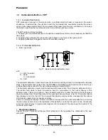
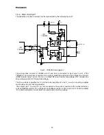
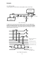
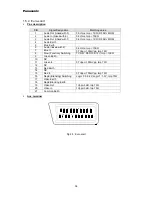
The deflection coil drive circuit part can be represented by the following figure 27
47
46
2
1
L302
L301
R302
V dri (-)
V dri (+)
I dri (+)
I dri (-)
I501
TDA8844
3
8
6
7
9
4
5
Vp
V0(guard)
V FB
Vi(FB)
V0(B)
GND
+V
CURRENT
SOURCE
I301
TDA8356
+
-
A
+
-
B
+
-
D
+
-
-
+
C
-I
S
+I
S
T
+I
T
-I
+Vp
+Vp
+Vp
Y
I
Deflection Coil
V0(A)
LY
R304
//
R305
I1
I2
Idiff
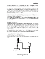
Fig.27 : TDA8356 block diagram
The vertical drive currents of TDA8844 pin 47 and 46 are connected to input pins 1 and 2 of the
TDA8356. The currents are converted into a voltage (called thereunder the drive voltage) by a resistor
(R302) between pins 1 and 2. Pin 2 is on a fluted DC level (internal bias voltage) Pin 1 includes the
drive voltage and the DC internal bias voltage.
The drive voltage is amplified by ’A’ and fed to two amplifiers ’B’ and ’C’, one is an inverting amplifier
and the other is a non inverting amplifier.
The outputs (pin 7: V
0(A)
and 4. V
0(B)
) are connected to the series connection of the vertical deflection
coil and feedback resistor. The voltage across feedback resistor is 134 via pin 9 to correction amplifier
’D’, to obtain a defection current which is proportional to the drive voltage.


