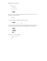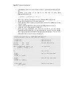
Appendix D: Breadboarding Rules
· Page 311
Appendix D: Breadboarding Rules
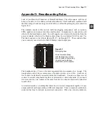
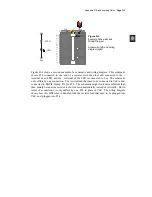
Look at your Board of Education or HomeWork Board. The white square with lots of
holes, or sockets, in it is called a solderless breadboard. This breadboard, combined with
the black strips of sockets along two of its sides, is called the prototyping area (shown in
Figure D-1).
The example circuits in this text are built by plugging components such as resistors,
LEDs, speakers, and sensors into these small sockets. Components are connected to each
other with the breadboard sockets. You will supply your circuit with electricity from the
power terminals, which are the black sockets along the top labeled Vdd, Vin, and Vss.
The black sockets on the left are labeled P0, P1, up through P15. These sockets allow
you to connect your circuit to the BASIC Stamp’s input/output pins.
P15
P14
P13
P12
P11
P10
P9
P8
P7
P6
P5
P4
P3
P2
P1
P0
X2
X3
Vdd
Vss
Vin
Figure D-1
Prototyping Area
Power terminals (black
sockets along top), I/O pin
access (black sockets along
the side), and solderless
breadboard (white sockets)
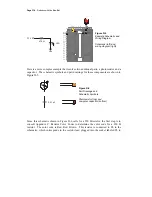
The breadboard has 17 rows of sockets separated into two columns by a trough. The
trough splits each of the seventeen rows of sockets into two rows of five. Each row of
five sockets is electrically connected inside the breadboard. You can use these rows of
sockets to connect components together as dictated by a circuit schematic. If you insert
two wires into any two sockets in the same 5-socket row, they are electrically connected
to each other.
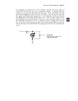
A circuit schematic is a roadmap that shows how to connect components together. It uses
unique symbols each representing a different component. These component symbols are
connected by lines to indicate an electrical connection. When two circuit symbols are


