Drawings
© PAT
Rev. - 12/18/00 // CSH.
190118_-.DOC
29
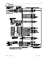
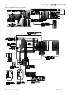
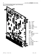
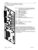
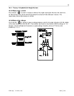
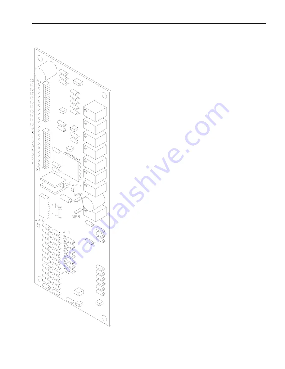
13.5 Central Unit Analog Input Module (Drawing 5)
BOARD P/N 024-352-300-020
X1:1-7 = ADC INPUT 0.5V...4.5V, Note: If channel adjustments
are made through the software and graphic console,
DO NOT adjust offset with P1-P7.
X1:8 = TEMP (0.5V + 10mV/
°
C)
X1:9 = VREFA = 5.000V reference
X1:10 = AGND (reference GND)
X1:11 = VREF+ = 5.0V power ADC
X1:12-15
= CH01-04, DIN1-4 / 10
X1:16 = CH05, +UBS / 10
X1:17 = CH06, HESIN(A2B) * 4
X1:18 = CH07, +9V * 4
X1:19 = CH08, VREFA / 2 = 2.500V
X1:20 = UKLEMM, app. VREFA, limits ADC input to 5.0V
MP1 = AGND
MP8 = +5V
MP1-7 = Input channels 1-7 0.5V/4mA…2.5V/20mA
MP14 = +13V REF02
MP16 -= HESIN input voltage
MP17 = app 5.4V clamp for inputs
The analog input module converts the sensor signals on
channels 1-7 to signals that will be processed at the CPU and
software. The incoming signal measured at the measuring points
(MP) will be 0.5V/4mA…2.5V/20mA. The analog input module
then converts the channel signals to 0.5V…4.5V, which can be
measured on X1:1 through X1:7.
The signal voltage can be measured at either point using ground
and the signal input.


