background image

Qty's

Remark

 No.

Summary of Contents for NT72563

Page 1: ...ification 3 Alignment Procedure 4 Scheme Diagram 5 Troubleshooting 6 Explode drawing This manual is t he latest at the time of printing and does not include the modification which may be made after th...

Page 2: ...electric shock to the person The exclamation point within an equilateral triangle is intended to alert the user to the presence of important operating and maintenance servicing instructions in the lit...

Page 3: ...to impact of any kind Be particularly careful not to damage the picture tube surface 9 Unplug this television set from the wall outlet before cleaning Do not use liquid cleaners or aerosol cleaners Us...

Page 4: ...ding conductors location of antenna discharge unit connection to grounding electrode and requirements for the grounding electrode 15 2 Note to CATV system installer Only for the television set with CA...

Page 5: ...cedurein youroperatinginstructions do not attempt any further adjustment Unplug the set and call your dealer or service technician 22 Whenever the television set is damaged or fails or a distinct chan...

Page 6: ...Picture Size 16 9 format 4 3 format Cinerama 16 9 Zoom 16 9 zoom up 14 9 zoom Picture enhancement technology On Off Speakers Integrated speakers Bottom side Audio Power Output THD 7 2 5W Auto Volume Y...

Page 7: ...NT72563 Factory Menu Spec V1 0 2017 10 17 Drafted by Checked by Approved By Kim yuan...

Page 8: ...TENTS 1 INTRODUCTION 1 2 OPEN THE FACTORY MENU METHOD 1 3 WHITE BALANCE 2 4 OTHER SUBMENU 3 5 NVM RESET SUBMENU 4 6 PRESET FACTORY CHANNEL SUBMENU 4 7 POWER ON MODE SUBMENU 4 8 USB CLONE UPDATE SUBMEN...

Page 9: ...tory mode data reset It will be done before shop initial if needroduct line HOTKEY will be di White Balance WhiteBalance Adjustment Other Set some TV setup NVM reset Do Clear NVM values Preset Factory...

Page 10: ...g key B Offset 0 255 Set B Offset by pressing key White Balance Init Do Press key to initialize RGB Gain Offset values Picture Related Press key to activate submenu Item Sub item Value Note Picture Re...

Page 11: ...fo Panel info RCU info Region info PSU info Running Time info Grey Ctl Grey Ctl Select Grey ctrl ON or OFF by pressing key to control picture menu Grey or not Update CI Credential Update CI Credential...

Page 12: ...starting sequence by pressing key ON Force TV to start STB Force TV to standby LAST Force TV to standby or to start depending on latest operation 8 USB Clone Update submenu Item Sub item Value Note US...

Page 13: ...dex V1 0 of 5 pages Name HDCP2 0 Upgrade Press ok key to upgrade HDCP2 0 key HDCP Upgrade Press ok key to upgrade HDCP key WideVine Upgrade Press ok key to upgrade WideVine Device id Upgrade Press ok...

Page 14: ...AWING CANNOT BE COMMUNICATED TO UNAUTHORIZED PERSONS COPIED UNLES S PERMITTED IN WRITING FORMAT DIN A1 H G F E D C A Index Lab Last saved TCLNO SBU DESIGNATION DESIGNATION MAIN1V5 GND GND ADJ OUT VIN...

Page 15: ..._QN DACOUT_R0 DACOUT_L0 VIFN VIFP HP AMP Audio Out HP Out Audio_Out HP_Out L201 L202 L203 L204 C281 C227 C283 C214 R210 R211 R212 R213 0R 10uH 0R 2200P NC 0 1u 330P 1K 47K 10R 100R GND GND GND R215 47...

Page 16: ...TRST LED_PWM_2 LED_SPI_CLK LED_YDIO NAND_CE_0 GPB_17 CI_HAD0 I2S_OUT_B_MCLK LED_PWM_3 LED_SPI_DO GPB_18 CI_HAD1 I2S_OUT_B_BCLK LED_PWM_4 LED_SPI_CS_0 GPB_19 CI_HAD2 I2S_OUT_B_WS LED_PWM_5 LED_SPI_CS_1...

Page 17: ...4K7 NC 15P CA08 CA05 15P NC NC 15P CA07 VDDRA NC1 RA GNDR PD ERROR SDATA LRCIN SDA SCL RESET VSS RB VDDRB VDDLB LB GNDL NC2 VDDLA LA VDD SA0 MCLK BCLK 12 11 10 9 22 24 23 21 20 19 18 17 8 7 6 5 4 3 2...

Page 18: ...HDMI_ARC STBC_GPI_15 MHL_CBUS MHL_CDS STBC_GPG_24 RXC_CLK RXC_CLK RXC_0 RXC_0 RXC_1 RXC_1 RXC_2 RXC_2 PWR5V_C STBC_GPI_4 HDMIC_SCL STBC_GPF4 HDMIC_SDA STBC_GPF5 NT72563M2 HDMI MHL US1 NT72563 Y19 W18...

Page 19: ...TXEC TXEC TXE3 TXE3 TXE3 TXE3 TXE3 TXE3 TXE3 TXE3 TXE4 TXE4 TXE4 TXE4 TXE4 TXE4 TXE0 TXE0 TXE0 TXE0 PANEL_VCC PANEL_VCC OUT OUT OUT 3 2 4 6 7 8 10 11 12 PANEL_VCC PANEL_VCC TXE3 TXE3 GND TXEC GND TXE2...

Page 20: ...LINE4 GND1 LINE1 NC3 ESD UN1 9 1 3 5 10 4 6 7 8 2 ESD5451R DN1 1 2 2R2 RN2 RXC TXC TX1P RX1N ETHERNET_TD ETHERNET_TD ETHERNET_RD ETHERNET_RD RX1P TX1N Must be differential 100ohm RJ45 Jack T T T T T...

Page 21: ...1 DDRS_A10 DDRS_A9 DDRS_A8 DDRS_A7 DDRS_A6 DDRS_A5 DDRS_A3 DDRS_A4 DDRS_A2 DDRS_A0 C189 0 1U DDRS_A14 DDRS_BA1 DDRS_BA2 DDRS_RASN DDRS_WEN DDRS_CLK DDRS_CLKN DDRS_DQS0 DDRS_DQS0B DDRS_BA0 DDRS_A13 DDR...

Page 22: ...BS18_IN_ STBC_GPI_14 STBC_GPG_27 STBC_UART_1_TX ARM_UART_B_TX ARM_UART_A_TX STBC_GPG_28 STBC_UART_1_RX ARM_UART_B_RX ARM_UART_A_RX STBC_GPG_29 STBC_UART_0_TX I2C_M0_SDA I2C_S_SDA SD_DAT0 STBC_GPG_30 S...

Page 23: ...DOUT_START DEMOD_EMERGENCY GPC_4 ARM_UART_B_TX INT_5 ARM_UART_A_TX GPC_5 ARM_UART_B_RX INT_6 ARM_UART_A_RX GPC_12 INT_7_BS0_ GPC_13 INT_8 GPC_14 INT_9 USB1_D USB1_D GPD_24 CI_RST TC_POL1 DISEQC_TX GPD...

Page 24: ...U C208 VDD33 MAIN2V5 MAIN3V3 MAIN2V5 CORE0V9 EMMC_VDD GND 120R L1113 GND 120R L1106 0 1U C215 GND VDD33 0 1U C175 2U2 C211 GND 0 1U C201 0 1U C195 0 1U C206 0 1U C200 0 1U C199 MAIN3V3 GND 2U2 C187 MA...

Page 25: ...70U 25V C832A 25V 470U C831A ZLED1 0R R795 0 47U C773 C775 1U C776 330P D830 MBR10150 1 3 2 R850 33R ZGND ZPCGND ZFB Z4 Z50V ZPGND Z5 Z6 ZHV ZN GND 1 12V 1 C835 0 1U C836 0 1U R833 1K Z7 U830 TL431 1...

Page 26: ...al Signal output from processor and input for panel O C Open Cell panel with source board BL Back Light light source for panel module LB LED Light Emitting Diode Bar light source for BL module VBL Vol...

Page 27: ...1 No power No power LED RC or Key can not turn on TV Power LED no light no change...

Page 28: ...2 No Display Black Panel Back light is OK sound is OK but no picture...

Page 29: ...3 No back light Power LED logic OK sound OK but no picture Different from No Display...

Page 30: ...4 No sound One or all signal source without sound...

Page 31: ...5 Signal source no function One or several source no function...

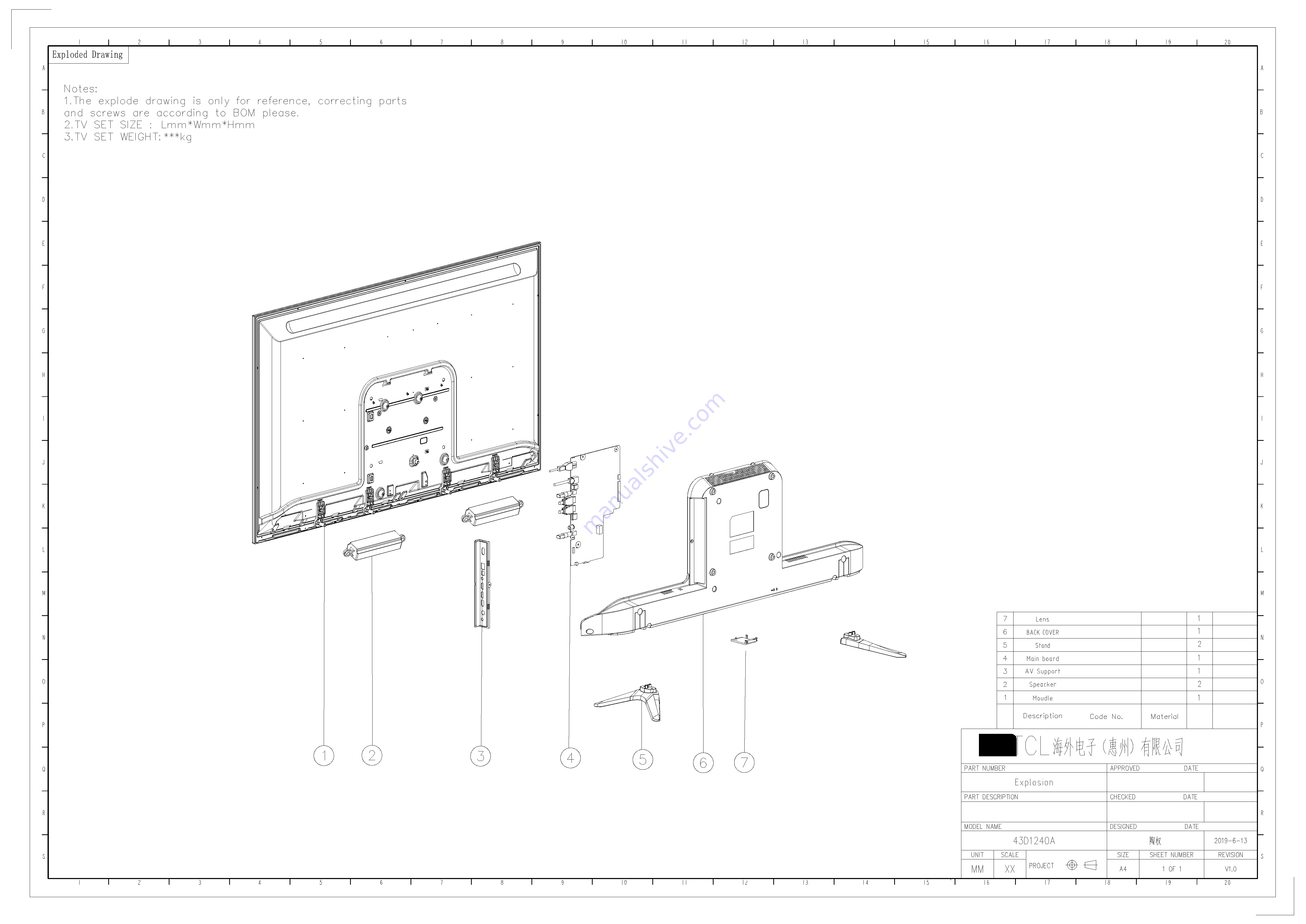
Page 32: ...Qty s Remark Exploded Drawing No...

Reviews: