Circuit Descriptions
7.
7.2
Power Supply
7.2.1
Power Supply Unit
Before checking other parts first check whether fuse on the
PSU is not broken. Always replace a defective fuse with one
with the correct specifications! This part is available in the
regular market.
Consult the Philips Service web portal for the order codes of the
boards.
In this manual, no detailed information is available because of
design protection issues.
The output voltages to the chassis are:
•
+3V3-STANDBY (Stand-by mode only)
•
+12V (on-mode)
•
+Vsnd (+24V) (audio power) (on-mode)
•
+24V (iBoard power) (on-mode)
•
Output to the display; in case of
- IPB: High voltage to the LCD panel
- PSL and PSLS (LED-driver outputs)
- PSDL (high frequent) AC-current.
7.2.2
Diversity
The diversity in power supply units is mainly determined by the
diversity in screen sizes.
7.2.3
Connector overview
Table 7-1 Connector overview
7.3
DC/DC Converters
The on-board DC/DC converters deliver the following voltages
(depending on set execution):
•
+3V3-STANDBY, permanent voltage for the Stand-by
controller, LED/IR receiver and controls; connector 1M95
pin 1
•
+12V, input from the power supply for TV550 common
(active mode); connector 1M95 pins 6, 7 and 8
•
+24V, input from the power supply for DVB-S2 (in active
mode); connector 1M09 pins 1 and 2
•
+1V1, core voltage supply for PNX85500; has to be started
up first and switched "off" last (diagram B03B)
•
+1V2, supply voltage for analogue blocks inside
PNX85500
•
+1V8, supply voltage for DDR2 (diagram B03B)
•
+2V5, supply voltage for analogue blocks inside
PNX85500 (see diagram B03E)
•
+3V3, general supply voltage (diagram B03E)
•
+5V, supply voltage for USB and CAM (diagram B03E)
•
+5V-TUN, supply voltage for tuner (diagram B03E)
•
+V-LNB, input voltage for LNB supply IC (item no. 7T50)
•
+5V-DVBS, input intermediate supply voltage for DVB-S2
(diagram B08A)
•
+3V3-DVBS, clean voltage for silicon tuner and DVB-S2
channel decoder
•
+2V5-DVBS, clean voltage for DVB-S2 channel decoder
•
+1V-DVBS, core voltage for DVB-S2 channel decoder.
A +12 V under-voltage detector
(see diagram B03C) enables
the 12V to 3.3V and 12V to 5V DC/DC converters via the
ENABLE-3V3-5V line, and the 12V to 1.8V DC/DC converter
via the ENABLE-1V8 line. DETECT2 is the signal going to the
Stand-by microcontroller and ENABLE-3V3n is the signal
coming from the Stand-by microcontroller.
Diagram B03D
contains the following linear stabilisers:
•
+2V5 stabiliser, built around item no. 7UCO
•
+5V-TUN stabiliser, built around items no. 7UA6 and 7UA7
•
+1V2 stabiliser, built around items no. 7UA3 and 7UA4.
Diagram B08A
contains the DVB-S2-related DC/DC
converters and -stabilisers:
•
a +24V under-voltage detection circuitry is built around
item no. 7T04
•
the switching frequency of the 24 to 14...20V switched
mode converter is 350 kHz (item no. 7T03 and +V-LNB
lines)
•
the output signal on the +V-LNB line goes to the LNBH23Q
(item no. 7T50)
•
the LNBH23Q (item no. 7T50) sends a feedback signal via
the V0-CNTRL line
•
the switching frequency of the +5V-DVBS to +1-DVBS
switched mode converter is 900 kHz (item no. 7T00)
•
a delay line for the +2V5-DVBS and +1V-DVBS lines is
created with item no. 3T03 (R=10k) and 2T06 (C=100n)
•
a 3.3V to 2.5V linear stabiliser is built around item no. 7T01
•
a 5V to 3.3V linear stabiliser is built around item no. 7T02.
Diagram B08B
contains the DVB-S2 LNB supply:
•
the +V-LNB signal comes from item no. 7T03
•
the V0-CTRL signal goes to item no. 7T03
•
the LNB-RF1 goes to the LNB.
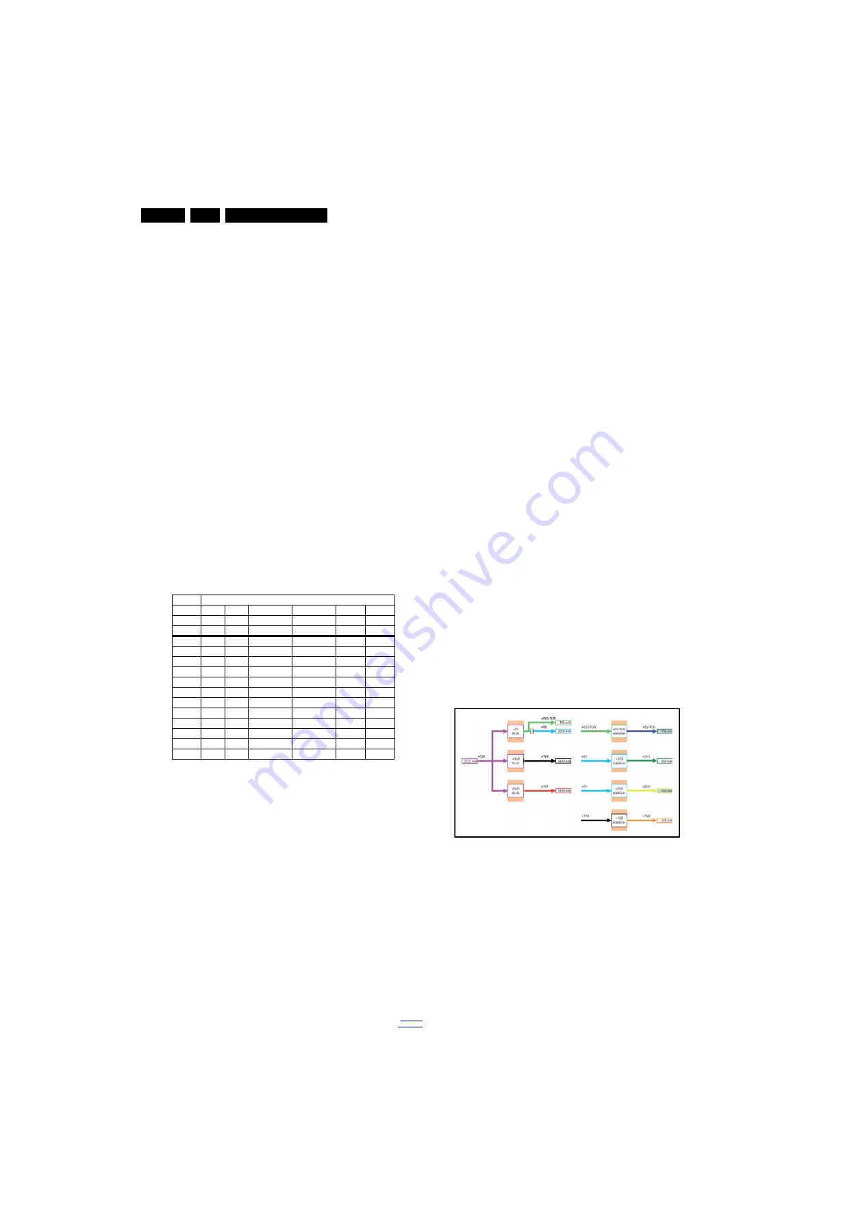
Figures gives a graphical representation of the DC/DC
converters with its current consumptions:
Figure 7-3 DC/DC converters xxPFL5xxx series
Connector
no.
1308
1311
1M95
1M99
1M09
1MP1
Descr.
Mains
Mains
to SSB
to SSB
Amb.
T-con
Pin
CN1
CN2
CN5
CN6
CN7
CN8
1
N
L’
3V3std
+12V
24Vb
+12V
2
L
L”
Stndby
+12V
24Vb
+12V
3
-
-
GND1
GND1
GND1
n.c.
4
-
-
GND1
GND1
GND1
GND1
5
-
-
GND1
BL_ON_OFF
-
GND1
6
-
-
+12V
DIM
-
-
7
-
-
+12V
Boost
-
-
8
-
-
+12V
n.c.
-
-
9
-
-
+Vsnd
POK
-
-
10
-
-
GND_SND
-
-
-
11
-
-
n.c.
-
-
-
12
-
-
-
-
-
-
1
8
770_225_100127.ep
s
100219


