background image

Circuit Descriptions, Abbreviation List, and IC Data Sheets

EN 94

LC4.9U AA

9.

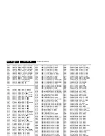
e.g. service mode (a DST-emulator is 
available in ComPair)

DTS

Digital Theatre System; A multi-
channel surround sound format, 
similar to Dolby Digital

DVD

Digital Versatile Disc

EEPROM

Electrically Erasable and 
Programmable Read Only Memory

EPLD

Erasable Programmable Logic Device

EPG

Electronic Program Guide: system 
used by broadcasters to transmit TV 
guide information (= NexTView)

EU

Europe

EXT

EXTernal (source), entering the set by 
SCART or by cinches (jacks)

FBL

Fast BLanking; DC signal 
accompanying RGB signals. To blank 
the video signal when it is returning 
from the right side of the screen to the 
left side. The video level is brought 
down below the black video level

FBL-SC1-IN

Fast blanking signal for SCART1 in

FBL-SC2-IN

Fast blanking signal for SCART2 in

FBL-TXT

Fast Blanking Teletext

FM

Field Memory; A memory chip that is 
capable of storing one or more TV 
picture fields / Frequency Modulation; 
A technique that sends data as 
frequency variations of a carrier signal

FMR

Radio receiver that can receive the FM 
Band 87.5 - 108 MHz

FRC

Frame Rate Converter

FRONT-C

Front input chrominance (SVHS)

FRONT-DETECT

Control line for detection of 
headphone insertion, Service Mode 
jumper, power failure detection

FRONT-Y_CVBS

Front input luminance or CVBS 
(SVHS)

G-SC1-IN

Green SCART1/EXT1 in

G-SC2-IN

Green SCART2/EXT2 in

G-TXT

Green teletext

H

H_sync to the module 

HA

Horizontal Acquisition; horizontal sync 
pulse

HD

High Definition

HP

HeadPhone

I

Monochrome TV system. Sound 
carrier distance is 6.0 MHz. VHF- and 
UHF-band

I

2

C

Integrated IC bus

I

2

S

Integrated IC Sound bus

IC

Integrated Circuit

IF

Intermediate Frequency

Interlaced

Scan mode where two fields are used 
to form one frame. Each field contains 
half the number of the total amount of 
lines. The fields are written in "pairs", 
causing line flicker.

IR

Infra Red

IRQ

Interrupt ReQuest

Last Status

The settings last chosen by the 
customer and read and stored in RAM 
or in the NVM. They are called at start-
up of the set to configure it according 
to the customer's preferences

LATAM

LATin AMerica

LC04

Philips chassis name for LCD TV 2004 
project

LCD

Liquid Crystal Display

LED

Light Emitting Diode; A semiconductor 
diode that emits light when a current is 
passed through it

LINE-DRIVE

Horizontal (line) deflection drive signal 
(for the Line transistor)

L/L'

Monochrome TV system. Sound 
carrier distance is 6.5 MHz. L' is Band 
I, L is all bands except for Band I

LS

LoudSpeaker

LVDS

Low Voltage Differential Signalling, 
data transmission system for high 
speed and low EMI communication.

M/N

Monochrome TV system. Sound 
carrier distance is 4.5 MHz. M= 525 
lines @ 60 Hz, N= 625 lines @ 50 Hz

MOSFET

Metal Oxide Semiconductor Field 
Effect Transistor

MPEG

Motion Pictures Experts Group. An 
ISO/IEC body that has given its name 
to an image compressing scheme for 
moving video

MSP

Multi-standard Sound Processor: ITT 
sound decoder

MUTE

MUTE Line

NC

Not Connected

NICAM

Near Instantaneously Companded 
Audio Multiplexing; This is a digital 
sound system, mainly used in Europe

NTSC

National Television Standard 
Committee. Colour system used 
mainly in North America and Japan. 
Colour carrier NTSC M/N = 3.579545 
MHz, NTSC 4.43 = 4.433619 MHz 
(this is a VCR norm, it is not 
transmitted off-air)

NVM

Non Volatile Memory; IC containing 
data such as alignment values, preset 
stations

O/C

Open Circuit

ON/OFF LED

On/Off control signal for the LED

OSD

On Screen Display

PAL

Phase Alternating Line. Colour system 
used mainly in Western Europe 
(colour carrier = 4.433619 MHz) and 
South America (colour carrier PAL M = 
3.575612 MHz and PAL N = 3.582056 
MHz)

PC

Personal Computer

PCB

Printed Circuit Board (or PWB)

PIG

Picture In Graphic

PIP

Picture In Picture

PLL

Phase Locked Loop. Used, for 
example, in FST tuning systems. The 
customer can directly provide the 
desired frequency

Progressive Scan

Scan mode where all scan lines are 
displayed in one frame at the same 
time, creating a double vertical 
resolution.

PWB

Printed Wiring Board (also called PCB 
or CBA)

RAM

Random Access Memory

RC

Remote Control transmitter

RC5 or 6

Remote Control system 5 or 6, the 
signal from the remote control receiver 

RGB

Red, Green, and Blue colour space; 
The primary colour signals for TV. By 
mixing levels of R, G, and B, all colours 
(Y/C) are reproduced

RGBHV

Red, Green, Blue, Horizontal sync, 
and Vertical sync

ROM

Read Only Memory

SAM

Service Alignment Mode

SC

SandCastle: two-level pulse derived 
from sync signals

SC-IN

SCART in

SC-OUT

SCART out

S/C

Short Circuit

SCART

Syndicat des Constructeurs 
d'Appareils Radiorécepteurs et 

Summary of Contents for 32-LCD HDTV MONITOR FLAT TV DIGITAL CRYSTAL CLEAR 32PF5320

Page 1: ...Block Diagrams Test Point Overviews and Waveforms Wiring Diagram 42 FHP 23 Wiring Diagram 42 SDI 24 Block Diagram Supply 42 FHP LGE 25 Block Diagram Video 26 Block Diagram Audio 27 I2C Overview 28 Supply Line Overview 29 SSB MUX Sync Interface B13 54 64 73 SSB Top Connectors B16 55 64 73 SSB Side Connectors B17 56 64 73 SSB ADC B18 57 64 73 SSB Columbus B19 58 64 73 SSB EPLD B20 59 64 73 SSB EPLD ...

Page 2: ... M N 3 58 4 43 Supported computer formats VGA 640x480 SVGA 800x600 XVGA 1024x768 Supported video formats 640x480i 1fH 720x576i 1fH 640x480p 2fH 720x576p 2fH 852x480p 2fH 1280x720 3fH 1920x1080i 2fH Presets channels 125 presets Tuner bands VHF UHF S band 1 2 Connection Overview Note The following connector colour abbreviations are used acc to DIN IEC 757 Bk Black Bu Blue Gn Green Gy Grey Rd Red Wh ...

Page 3: ...ta channel j 4 D1 Data channel j 5 Shield Gnd H 6 D1 Data channel j 7 D0 Data channel j 8 Shield Gnd H 9 D0 Data channel j 10 CLK Data channel j 11 Shield Gnd H 12 CLK Data channel j 13 n c 14 n c 15 DDC_SCL DDC clock j 16 DDC_SDA DDC data jk 17 Ground Gnd H 18 5V j 19 HPD Hot Plug Detect j 20 Ground Gnd H PC VGA DVI 2 Video 2fH RGB YPbPr In Figure 1 4 VGA Connector 1 Video Red Pr 0 7 VPP 75 ohm j...

Page 4: ...o pins of the Mains AC Power plug Check the cabinet for defects to prevent touching of any inner parts by the customer 2 3 Notes 2 3 1 General Measure the voltages and waveforms with regard to the chassis tuner ground H or hot ground I depending on the tested area of circuitry The voltages and waveforms shown in the diagrams are indicative Measure them in the Service Default Mode see chapter 5 wit...

Page 5: ...rom old tin and re solder with new tin Use only original spare parts listed in the Service Manuals Not listed standard material commodities has to be purchased at external companies Special information for lead free BGA ICs these ICs will be delivered in so called dry packaging to protect the IC against moisture This packaging may only be opened shortly before it is used soldered Otherwise the bod...

Page 6: ...Directions for Use EN 6 LC4 9U AA 3 3 Directions for Use You can download this information from the following websites http www philips com support http www p4c philips com ...

Page 7: ...Dressing 4 2 Service Positions 4 3 Assy Panel Removal 4 4 Set Re assembly Notes Figures below can deviate slightly from the actual situation due to the different set executions Follow the disassembling instructions in described order 4 1 Cable Dressing Figure 4 1 Cable dressing F_15430_043 eps 080605 ...

Page 8: ...round the outer rim tapping screws around the connector plate 3 Remove the four mushrooms from the rear cover 4 Lift the metal rear cover from the set Make sure that wires and flat foils are not damaged 4 3 2 Speaker Compartment Cover After removing the metal rear cover you gain access to the Speaker Compartment covers 1 Remove all T10 screws 1 around the outer rim of the cover see Figure Speaker ...

Page 9: ... assy 3 Remove the panel from its bracket 3 by pushing against the front side of the side I O cinch connectors Figure 4 7 Side I O panel removal When it is defective replace the whole unit 4 3 4 LED Panel Figure 4 8 LED panel 1 Remove the fixation screws 1 and take the panel out of its brackets 2 Disconnect the cable 2 from the panel 4 3 5 Keyboard Control Panel F_15430_048 eps 100605 2 1 3 F_1542...

Page 10: ...r shield Notice that this cable is very fragile 2 Remove all other cables 2 from the SSB board see Figure SSB board cover shield including the grounding 4 3 7 Small Signal Board Figure 4 12 SSB 1 Remove the two fixation screws 1 that secure the SSB board on the lower part of the SSB shielding see Figure SSB 2 Remove the SSB 4 3 8 Power Supply Panel F_15430_049 eps 100605 2 2 1 3 3 F_15270_075 eps ...

Page 11: ...o Amplifier Panel Figure 4 14 Class D audio amplifier panel 1 Disconnect all cables 1 from the panel 2 Pinch the plastic fixation clamps 2 firmly between your fingers and pull the panel upwards 3 Take the panel out of its brackets 3 F_15430_051 eps 100605 3 2 1 ...

Page 12: ...e Main Supply board Mains cable at the Main Supply board Side I O cable at SSB side fragile connector Cable at LED panel Keyboard cable at SSB side Audio Amplifier supply cable at the Main Supply board Loudspeaker cables incl ferrites at the Audio panel 4 Lift the metal frame together with all PWBs from the display panel see figure Frame lift 5 After removal of the frame lift the PDP from the set ...

Page 13: ...plate 1 Remove the PDP as described earlier 2 Remove the T10 screws 1 from the mounting frame 3 After removal of the frame you can lift the glass plate from the set Figure 4 17 Glass plate removal 4 4 Set Re assembly To re assemble the whole set execute all processes in reverse order F_15400_119 eps 200505 1 ...

Page 14: ...hassis It offers the possibilities of structured troubleshooting error code reading and software version read out for all chassis Minimum requirements for ComPair a Pentium processor a Windows OS and a CD ROM drive see also paragraph ComPair 5 2 1 Service Default Mode SDM Purpose To create a predefined setting for measurements to be How to Enter To enter SDM use one of the following methods Press ...

Page 15: ...imer The run timer counts normal operation hours but does not count standby hours 2 AAABCD X Y This is the software identification of the main microprocessor A the project name LC04 x B the region E Europe A Asia Pacific U NAFTA L LATAM C the software diversity Europe T 1 page TXT F Full TXT V Voice control LATAM and NAFTA N Stereo non dBx S Stereo dBx Asian Pacific T TXT N non TXT C NTSC ALL regi...

Page 16: ... will appear 8 Displays the detected Audio e g stereo mono 9 Displays the picture setting information 10 Displays the sound setting information How to Exit To exit CSM use one of the following methods Press the MENU STATUS EXIT or POWER button on the remote control transmitter Press the POWER button on the television set 5 3 Problems and Solving Tips Related to CSM 5 3 1 Picture Problems Note The ...

Page 17: ...all repair information is directly available When ComPair is installed together with the Force SearchMan electronic manual of the defective chassis schematics and PWBs are only a mouse click away Specifications ComPair consists of a Windows based fault finding program and an interface box between PC and the defective product The ComPair interface box is connected to the PC via a serial or RS 232 c...

Page 18: ...ComPair release 2004 1 or later on your PC engine version 2 2 05 For every TV type number and screen size one must choose 5 5 Error Codes The error code buffer contains all errors detected since the last time the buffer was erased The buffer is written from left to right When an error occurs that is not yet in the error code buffer it is displayed at the left side and all other errors shift one po...

Page 19: ...s followed by a pause of 1 5 seconds 1 long blink of 1 5 seconds to finish the sequence The sequence starts again with 12 short blinks 5 7 Fault Finding and Repair Tips Notes It is assumed that the components are mounted correctly with correct values and no bad solder joints Before any fault finding actions check if the correct options are set 5 7 1 NVM Editor In some cases it can be handy if one ...

Page 20: ...y software 0 Total Dec Values 56 Total Hex Values 38 Byte 1 175 dec 0 PSE PSE 0 1 OPC OPC 0 2 PRIS PRIS 0 3 CONTINUOUS FACTORY Continuous factory mode 1 4 WHITE PATTERN ON Last colour pattern status in factory mode 0 5 SDM MODE Service default mode on off 0 6 SAM MODE Service Align mode on off 0 7 SVMA Scavem On Off 0 Total Dec Values 8 Total Hex Values 08 Byte 2 176 dec 0 MUTE STATUS Mute status ...

Page 21: ...SK Dynamic skin tone angle on off 0 Total Dec Values 78 Total Hex Values 4E Byte 6 180 dec 0 LTI status LTI last status 0 1 Inc_Life_Time Inc_Life_Time 0 2 PC_Mode PC_Mode 0 3 HD_Mode HD_Mode 0 4 Tact_Switch Tact_Switch 0 5 Set_In_Special_Stby Set_In_Special_Stby 0 6 Hotel_OSDDisplay Hotel_OSDDisplay 0 7 Hotel_MonitorOut Hotel_MonitorOut 0 Total Dec Values 0 Total Hex Values 00 Byte 7 181 dec 0 Ho...

Page 22: ...ed for the digital video path Hercules output whereas the analogue RGB input analogue input of the scaler is only used for teletext This means that no mixed mode video plus teletext simultaneously is possible If there is sound and teletext but no video and user menu blank screen the digital path Hercules ADC Columbus Scaler is faulty If there is sound but no teletext the back end part Scaler LCD p...

Page 23: ...VERTER INVERTER RIGHT SPEAKER LEFT SPEAKER PDP POWER SUPPLY E CONTROL BOARD 3P 1M01 3P 1K02 6P 1K00 11P 1M36 9P 1J04 10P 1J00 11P 1J01 11P 1M46 10P 1M03 7P 1M02 10P 0323 7PP 1002 8P13 CN32 8P13 CN22 2P3 0308 AC INLET F_15451_001 eps 151205 8735 8736 8102 8152 8120 8136 8146 8103 8199 8900 8101 1107 3P Tuner 8150 31P 1P07 3P LVDS CONNECTOR B A SSB 3P4 1M10 10P C561 8323 9P 0311 9P DISPLAY 8202 1101...

Page 24: ...ER RIGHT SPEAKER LEFT SPEAKER PDP POWER SUPPLY E CONTROL BOARD 3P 1M01 3P 1K02 6P 1K00 11P 1M36 9P 1J04 10P 1J00 1M03 11P 1J01 1M46 31P 1J04 11P 1M46 10P 1M03 7P 1M02 7P 1M02 31P LVDS CONNECTOR 10P CN06 8P CN07 10P P5 4P P6 4P 1K00 8P P1 2P3 CN308 AC INLET F_15430_052 eps 281105 8735 8736 8102 8152 8120 8136 8146 8150 8103 8199 8900 8101 Tuner 1107 3P 1103 3P 1101 3P Compair UART WIRING 42 SDI ...

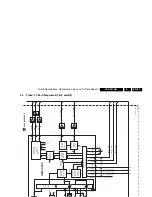
Page 25: ...0 30V 3111 VRA VSA_CONTROL 2121 1200 T2A 7212 TEA1507P 1 VCC DRIVE 8 3 DRAIN CONTROL 6 GND CTRL 5220 1 14 8 6226 VCC 5225 IN OUT COM 7230 6230 5229 8V6 3228 3229 K A R 1 3 2 7502 K A R 1 3 2 7502 3224 4 7217 3218 3149 7200 3206 3209 5 7 3220 6211 4 DEMAG 3213 3214 6213 VCC_GO 7202 3202 3203 6202 7 2 1260 T2A 30V 7260 L4973V3 3 REGULATOR 8 VCC 5260 3 5268 12V OUT 7050 VS 7052 3053 T SEQUENCE DISCHA...

Page 26: ...SC1_R_CVI_Pr_IN SC1_G_CVI_Y_IN R_PR ADC G_Y ADC B_PB ADC 19 PC_HD_DET HDMI PC D 6 7 5SW_a VTUN 1 2 1 2 3 7436 2 4 3 7436 1 3 1 N C EF 7L01 EF 7L03 EF 7L02 7L04 MST9883C A D CONV COL_A COL_D 7M00 T6TU5XBG COLUMBUS DIGITAL COMB FILTER DRAM 512Kx16x2 7M01 MSM56V16 2V5_DDR 95 F_15420_049 eps 251005 48 43 54 30 31 56 57 SCL SDA COL_Do 1 7 COL_YB 1 7 7E00 1 13 3 5 2 12 15 14 4 SD_HD_SEL 10 11 C3 SOG BIN...

Page 27: ...UDIO IN L R CVI 1 AUDIO IN L R AV3_HDMI AUDIO_SEL 10 11 AUDOUTLSR AUDOUTLSL 1K04 10 10 1M36 11 11 HP_LOUT HP_ROUT HEADPHONE SOUND L HEADPHONE OUT SOUND R HEADPHONE OUT MUTE OUT_MUTE POWER_DOWN SOUND_ENABLE 4211 4212 1J04 1M52 1 1 1M52 3 3 8 8 SOUND ENABLE_1 7606 7601 TS482ID 1 7 2 6 1010 2 3 5 7 7 DETECT EXT_MUTE 2 1 9 10 7602 74HC08PW B16 B2 B2 6 8 OUT_MUTE 3 5 9 9 POR_AUDIO B5 3628 3629 13 12 5V...

Page 28: ...2 1802 1 JTAG_TDI_SDA JTAG_CLK_SCL AF7 AD6 3V3IO 3838 3837 JTAG I2C FSDATA FSADDR OCMDATA OCMADDR 7 57 56 7L04 MST9883C ANALOG INTERFACE ERR 7 3L19 3L20 7L07 7L06 3V3SWB 3L36 3L37 3V3SWB A15 B15 7M00 T6TU5XBG COLUMBUS CTRL ERR 11 3M14 3M15 ERR 17 T2 R2 7N02 EP1C12F256C8N EPLD BANK 4 ERR 16 4N21 4N22 1N02 2 3 4 FOR DEVELOPMENT USE ONLY SDA SCL 1 3V3SW 3N46 3N47 7A00 PCA9515ADP 1P07 1G50 31 30 3 2 6...

Page 29: ...SW 5VHDMI 5VHDMI 3V3SW 3V3SW 5VSWI 5VSWI 5VSWI 5VSWI DDC_5V 5F03 6F00 1 1F00 DVI_5V 3F20 6F01 5VSW 5VSW 3V3STBY 3V3STBY 5VSW 5VSW 5VSWIA 5VSWIA 3V3SWB 7K05 IN OUT COM 3V3SW 3V3SW 3V3SWA 5M03 5VSWI 5VSWI 5VSWIA 5M04 3V3SW 3V3SW 3V3 IO 3V3 IO 3V3SW 3V3SW 3V3 IO LVDS_VCC LVDS_VCC 1V5 7P01 IN OUT COM 5P01 5P02 5P03 1V5 PLL 1V5 INT 1K00 5 5K00 1K04 7 5K01 3V3STBY_1 5VSW_1 1 1J01 1M46 2 3 4 5 6 7 8 9 10...

Page 30: ...8 E7 I501 E3 I502 E4 I503 E5 I519 F9 I520 A6 6W7 680K 3507 I526 H11 I527 H10 RELAY CONTROL EMC HOLE 1405 1005 750mA F 0309 0 106451 1 9003 9004 3472 1K0 16V 100u 2541 I504 I513 9V_STBY_SW I509 I512 6460 BAS316 2001 470n 400V_HOT 500V B2P VA BF 0308 1 2 DSP 501N 1402 F503 3463 10K GROUND F508 I416 I406 1404 EMC HOLE I407 2003 470n 100 230VAC2 F500 I411 100u 2532 16V F501 2503 47u 400V 3400 2322595 ...

Page 31: ... D8 I347 D8 I348 D8 I349 C9 I350 D9 I351 D9 I352 D10 I382 F1 15K 3074 I307 I344 16V 10u 2398 2387 100u 16V 47K 3398 3397 47K 47K 3394 47K 47K 3392 3393 1K0 3390 100R 3386 3399 3396 5K6 3320 10K 47K 3381 BAS316 6367 7004 P0102BL 560R 3356 10K 3353 7366 4 12 13 14 4 11 I381 LM324 5V_STBY_SW I380 100K 3395 I305 LM339P 5 4 2 3 12 7348 BC847BW 7330 3 BC857BW 7391 10K 3341 3342 10K BC847BW 7352 6335 F36...

Page 32: ...7 I613 E7 I614 B8 I662 H12 I663 G1 I664 I6 I665 I7 I666 I6 I667 I7 I668 I7 I616 G5 I617 G2 I618 H4 I619 H4 I620 H5 I621 G4 I633 H1 I634 B6 I641 E8 I642 E10 I643 G7 I644 G8 I645 G8 I646 G8 NFR25 NFR25 I660 330K 3684 I659 6640 SS14 I657 I645 I656 I653 I654 I602 I651 I650 3677 47K 3673 1K0 F601 I632 3671 10K 10n 2675 500V F605 50V 2613 1n0 BZG03 C18 6609 I642 I649 3621 2603 I615 I667 I668 BC369 7608 ...

Page 33: ...14 86V 6V 19382 19382 HOT U14 E6 0204 H9 1000 G6 F G 2008 F3 2009 E5 1008 G9 1 4 3 2070 1n0 TCET1102 G 7002 BAS316 6005 I020 I018 4K7 3012 6R8 3021 F293 I059 50V 2024 3n3 3043 4K7 6034 BAS316 3005 27K I074 F004 I079 2016 50V 2u2 100n 2047 6044 STTH2003C 1 3 2 200V 2028 220p 47p 2037 F295 GND4 F292 F007 F290 I039 3059 56K 3070 10K 6010 BAS316 50V 2010 10n 10K 3013 9007 BCP56 7013 6003 BZX384 C33 50...

Page 34: ...169 H8 I245 I8 I246 B6 H I I134 B10 I135 C6 I136 B10 1M10 I235 G11 I236 G9 19382 39812 VA 6 1 I138 A9 I139 A7 I140 B8 I141 A8 F 6216 H8 I142 A6 0V5 1J01 G H I114 E2 I115 D2 I116 D2 I117 D3 7060 2 B11 0V5 DISPLAY RES I118 D4 I120 D8 I121 D7 I122 D10 I123 D9 I221 19382 NFR25 I243 I11 I244 I3 0R51 3145 BZX384 C18 6061 BYW29EX 200 6120 3062 1K0 12V 10K 3147 12V 1K0 3142 50V 2227 100p 3220 33R I114 470...

Page 35: ...00 F5 3202 F6 3203 G6 3204 F5 3205 F5 3206 F5 3207 F5 3208 F5 3209 F5 3210 E8 3212 F6 3213 F6 3214 F6 3215 F6 3216 F6 3217 F6 3218 F6 3219 F5 3220 G6 3224 E8 3225 E8 3226 E8 3228 E8 3229 E8 3260 F8 3261 F8 3262 G8 3263 G8 3264 G8 3265 G8 3268 G8 3269 G7 3292 B8 3300 E6 3301 E6 3304 G7 3306 G7 3307 G7 3308 G6 3311 F8 3312 G7 3313 G7 3317 G7 3320 G7 3321 G7 3322 G7 3323 G7 3324 G7 3325 F7 3326 G7 33...

Page 36: ...EN 36 LC4 9U AA 7 Circuit Diagrams and PWB Layouts Layout PDP FHP Supply Part 1 Top Side E_16040_036a eps 161205 Part 1 ...

Page 37: ...Circuit Diagrams and PWB Layouts EN 37 LC4 9U AA 7 Layout PDP FHP Supply Part 2 Top Side Part 2 E_16040_036b eps 161205 ...

Page 38: ...EN 38 LC4 9U AA 7 Circuit Diagrams and PWB Layouts Layout PDP FHP Supply Part 3 Top Side E_16040_036c eps 161205 Part 3 ...

Page 39: ...Circuit Diagrams and PWB Layouts EN 39 LC4 9U AA 7 Layout PDP FHP Supply Part 4 Top Side E_16040_036d eps 161205 Part 4 ...

Page 40: ...EN 40 LC4 9U AA 7 Circuit Diagrams and PWB Layouts Layout PDP FHP Supply Bottom View 3104 303 5016 1 E_16040_037 eps 271005 ...

Page 41: ...NC2 10 4 SCL 5 1102 33V 9 5V 7 8 ADC AGC 1 AS 3 IFOUT 11 TUNER UV1318ST AIH MK3 47K 3114 6107 BZX384 C6V8 I106 4102 F103 F105 5VSW 5VSW_b 2103 10n F110 6101 BZX384 C6V8 3104 10K 4104 5VSW I108 5107 F108 3112 18K 10n 2106 16V 22u 2109 2101 100u 16V 4112 4109 2112 1n0 100R 3123 100R 3101 100R 3102 4107 F106 3105 1K0 3118 150K 10n 2102 1 2 3 4 5 6 3103 10K 1103 BAS316 6103 5105 2114 1u0 I109 4106 I11...

Page 42: ...14 B6 2216 B6 2218 A7 2219 A7 2220 B7 2221 A7 2223 B8 2224 C8 2225 B10 2226 C10 2227 B11 2228 C5 2229 C5 1V4 B23 B15 B15 B23 2 2V9 B7 B1 B9 6 B17 B5 HERCULES 0V B7 A B1 B7 10 0V 2201 A3 2202 B3 2203 D2 B4 RES RES 1V6 3V9 RES B15 B23 B5 RES H RES G B15 B13 B15 B23 B8 RES C 13 3V2 B17 8 I 1V9 1V9 3 B13 0R 2V7 B15 B23 0V 1201 B7 1202 G10 3 4 5 6 7 8 9 10 11 12 13 A B C D E F G H I J F233 2255 100n 22...

Page 43: ...39 E2 1440 D9 6 4436 A6 4436 I449 12VSW I450 100R I454 3462 14 8 3V3SW 74LVC14APW 7436 4 9 7 3458 100R I453 3454 100R 4441 3461 100R 3453 100R 4437 5V 3V3SW 14 4 74LVC14APW 7436 2 3 7 74LVC14APW 7436 5 11 7 14 10 2447 10p I452 B3B PH SM4 TBT LF 1441 1 2 3 4 5 3V3STBY 3V3STBY 4440 4439 I451 5431 1N4148 6431 3V3SW 3V3SW 7 14 12 3463 74LVC14APW 7436 6 13 3455 100R 6 3V3SW 7436 3 5 7 14 74LVC14APW 100...

Page 44: ...14 C9 8 7506 B8 2V3 2V5 2V6 2V6 7501 A1 COUNTER RES 10 A 2506 C10 2V6 C 2502 B2 2504 B8 2505 B9 2V6 4503 F2 6 5V3 2503 D2 2509 F7 I505 E2 4504 F3 0V2 2507 D10 2V6 5V3 4 7502 A3 3502 47K 5VD 5VD 4504 5501 1u0 5VSWI 6 7 13 9 16 VCC GND 8 14 15 1 2 3 4 5 7501 M74HC590T 11 12 10 5VD F505 4513 I505 3501 470R 4503 470p 2507 5VD F503 1 19 18 17 16 15 14 13 12 20 2 3 4 5 6 7 8 9 10 11 74HC573PW 7506 1 19 ...

Page 45: ...2 B7 3620 E8 3621 E8 3623 F5 7602 4 D6 PDTA143ET 3629 E5 RES 4616 C4 RES RES 3628 D5 3630 E5 4617 C5 4618 A4 TS482IDT 7601 2 5 I618 F601 10K 4601 3626 3V3STBY 39R 3633 4621 3632 39R 4618 10K 3619 4613 4611 I607 I604 22K 3609 1u0 2608 2619 F602 47u 4609 4610 10V 1 2 7 14 3 2613 1u0 7602 1 74HC08PW 10K 3620 1u0 2603 3615 10K 4614 I617 3605 3612 22K 22K I619 5V 4602 4619 I603 2605 1u0 3617 1K0 3V3SW ...

Page 46: ...V5 5V4 FROM SCALER FOR LCD ONLY 1R0 FOR UFD ONLY 3752 16V 47u 2738 5730 10u SUP_GND1 I751 F736 5738 I712 1 2 3 6709 SS14 5 6 7 8 4 2 3 4 5 6 7 7758 SI4433DY 1751 1 100R 3761 22u 2762 16V I755 3760 100R 8VSW_TV SUP_GND3 1K0 3759 IS 1 SWC 2 SWE 3 TIMC 6 VCC SUP_GND1 IPK OSC REFERENCE REGULATOR 5 CIN_NEG 8 DCOL 4 GND 7 7752 MC34063AD S R Q SUP_GND2 I716 4n7 2755 15K 3742 2761 1u0 25V 1 2700 SUP_GND1 ...

Page 47: ...W COL R 7210 V V V V V TRA SIG SM BC847BW COL R 7217 V V IC SM TDA15011H N1BD0 PHSE Y 7217 V V V V V IC SM TDA15021H N1B91 PHSE Y 7219 V V V IC SM 74HC4053D PHSE R Item 26 32PFxxxx AP NAFTA LT EU AP DVB sets LC4 3E LC4 9x LC4 8x LC4 3A China 26PF4310 10 Description 2449 V V V CER2 0402 Y5V 16V 100N COL 3432 V RST SM 0402 2K7 PM5 COL 3458 V V V RST SM 0402 100R PM5 COL 3459 V V V RST SM 0402 100R P...

Page 48: ...3_FPLL F3 VSSA33_RPLL ACS_RSET_HD K2 G3 TCLK J3 VDDA33_DDDS G1 VDDA33_FPLL 100n 2812 GM1501 LF BD 7801 11 CLK SYN 4801 3820 10K I801 3819 3834 10K 2 7 3803 2 22R 3802 4 4 5 2824 22R 2 7 22p 22R 3804 2 22R 3810 4 4 5 2811 100n 3V3_IO 1 8 22R 3 6 22R 3813 1 2V5_DDR 3813 3 22R 3809 1 1 8 I805 I804 100n 2806 1 8 22R 3808 1 2 7 14M31818 1801 SMD 49 22R 3813 2 3816 22R 100n 2814 100n 2816 2819 100n 22R ...

Page 49: ...C_IN3 D12 LBADC_RETURN 3902 7801 3 ADC 3V3SW 3V3STBY F909 5901 2924 100n 100n 2951 3901 2920 100n F904 2948 100n 2939 100n 100n 2908 100n 2915 F908 2931 100n B10 RX2n RX2p A10 B6 RXCn A6 RXCp 16V 47u 2904 D7 D11 N4 DVI_SCL GPI_07 N3 DVI_SDA GPI_08 B11 REXT B8 RX0n A8 RX0p B9 RX1n A9 RX1p C6 C8 C9 C10 C11 A7 A11 B5 B7 C7 7801 2 GM1501 LF BD DVI D6 D8 D9 D10 100R 3904 3903 100R F905 5907 1V8_DVI 295...

Page 50: ...6A01 4A06 2A13 100n BC847BW 7A03 3A14 4K7 4K7 3A11 10K 3A13 IA09 4A00 IA08 2A02 100p SHIELD1 DEGRN3 AC11 SHIELD2 DEGRN4 AD11 SHIELD3 DEGRN5 AE11 SHIELD4 DEBLU2 AE13 SHIELD5 DEBLU5 AD14 AF15 B2n DEBLU4 AE14 B2p DEBLU3 AF14 B3n DEGRN7 AF12 B3p DEGRN6 AF11 BCn DEGRN9 AF13 BCp DEGRN8 AE12 SHIELD0 DEGRN2 AF10 A3n GPIO_G06_B5 DORED7 AF19 A3p GPIO_G06_B4 DORED6 AE19 ACn GPIO_G06_B7 DORED9 AF20 ACp GPIO_G...

Page 51: ...2 92 99 25 59 67 73 79 86 58 16 46 66 85 27 93 15 35 65 96 2 95 8 14 22 89 90 91 39 40 41 42 43 44 87 88 84 3 4 6 7 60 61 94 52 38 20 21 74 75 77 78 80 81 1 83 69 71 72 9 10 12 13 100 17 18 28 23 56 24 57 97 98 63 64 68 48 49 50 51 45 29 30 26 55 53 54 K4D263238F UC50 1M X 32 X 4 SDRAM Φ 31 32 36 37 33 34 47 7B01 2B12 2V5_DDR 100n 100n 2B10 2B07 100n 3B02 10K 1 FB01 1 10K 3B01 2B09 100n 2B14 FSCLK...

Page 52: ...040B 55K1 3C06 1 10K 1 10K 3C04 2 2 7 3C17 10K 10K 3C09 3 3 6 100n 3 1 MR 2 SUB VCC 5 4 VOUT 2C02 PST596J 7C02 GND 8 3V3_IO 10K 3C07 1 1 3C20 1 8 5 3C04 1 10K 3C06 4 10K 4 10K 3C07 3 3 6 3C09 2 2 7 3V3SW FC08 1 8 10K 10K 3C09 1 2C03 100n 3V3SW 2 7 FC06 3C08 2 10K 3C12 5C00 8 FC04 1 FC07 3C16 1 2 7 FC00 3C10 2 10K 4 5 3V3_IO 3C08 4 10K 3C06 3 10K 3 6 2 7 3C06 2 10K 3C05 10K 3C11 10K 3C04 4 4 5 3C04...

Page 53: ...FD11 A7 2D21 B6 ID14 ID02 3D16 11 8 1 8 33R 33R 3D18 1 33R 4 5 5D00 3D17 4 3V3SW 2D03 10u ID13 2D10 1n0 3 6 3D17 3 33R ID18 2D14 1n0 ID00 2D19 1n0 FD00 100 34 31 ID04 91 97 96 84 83 32 30 29 17 40 64 58 55 72 9 18 73 19 20 87 86 92 68 39 38 37 36 63 62 61 60 59 69 54 53 52 51 50 49 48 44 43 42 47 56 67 79 22 24 25 80 23 70 26 3 4 46 28 45 57 66 78 21 77 76 81 16 41 65 99 101 33 71 27 75 2 13 10 5 ...

Page 54: ... 10 11 12 13 A B C D E F G H I IE12 3E01 100n 2E16 2E17 100n 56R 2E32 3E00 IE33 100n 3E13 330R 33p 2E07 100n 2E31 3V3SW 14 12 IE35 74LVC14APW 7E05 6 13 7 9 7 14 8 7E04 4 74LVC14APW 5VSWI 1u0 2E05 7E04 1 1 7 14 2 3E55 74LVC14APW 47K 2E04 1u0 FE12 FE05 4E10 47K 3E09 3E07 47K 3E08 47K 3E36 100R 3E41 100R 39R 3E29 3E44 100R 6E02 IE36 BZX384 C2V7 8 12 13 2 1 5 3 16 7 11 10 9 14 15 4 6 Φ 7E00 ADG733BRU ...

Page 55: ...FOR LCD FOR UFD ONLY 3V2 IJ03 A1 IJ04 A1 IJ05 A1 IJ12 A4 IJ13 E4 NC NC AMBIENT LIGHT FJ02 C1 FJ03 C1 3 4 5 6 7 FJ22 D7 FJ23 D7 FJ24 D7 3V3 FROM SCALER 1 2 1M46 1J03 E1 100p 2J21 FJ19 IJ01 FJ24 2J07 100p 4J01 10 11 2 3 4 5 6 7 8 9 1J01 1 FJ23 2J14 100p IJ08 5 6 7 8 9 IJ07 1J00 1 10 2 3 4 IJ12 2J29 100p 5 6 7 1J06 B7B PH K S LF 1 2 3 4 GND_AUDIO FJ20 100p 2J26 IJ04 2J27 100p FJ18 IJ06 FJ08 2J16 FJ10...

Page 56: ...D RES TOP SIDE KEYBOARD 4 FK11 B8 FK04 1K00 1 2 3 4 5 6 B6B PH K 2K13 100p FK02 5K02 1u0 2K02 10p FK09 68R 3K11 FK01 2K25 100p 4K04 15K 4 5 6 7 8 9 3K03 1 10 11 2 3 4K03 1K04 4K01 FK00 3K00 100R 4K06 2K24 100p 4K07 FK07 3V3STBY_1 2K22 100p 100p 2K21 10p 2K04 IK18 FK08 15K 3K06 100R 3K01 3K08 68R 100p 2K06 IK17 2u2 2K12 10K 3K02 FK03 100p 2K28 100p 2K23 5 6 7 8 9 14 15 16 17 18 19 2 20 3 4 1K03 1 1...

Page 57: ...7L08 C3 IL01 C5 IL02 C5 1V5 0R IL13 C7 IL12 C7 3L38 2 IL10 IL11 3L04 3L27 4 22R 3L37 3K3 2L23 100n 3V3SWB 1K0 3L12 16V 10u 2L30 5VSWIA 5VSWIA 3L16 3L26 3 22R 3K3 3L36 BC847BW 7L01 100n 2L10 IL04 4L04 3L25 1 22R 7L08 3L28 3 22R 150R 3L11 330R 3L10 3L13 5VSWIA IL05 3L15 2L24 100n 2L35 2L18 82n IL19 3L28 4 22R IL18 2L04 IL02 100n 47n 2L13 3L01 3L32 7L02 BC847BW 2K2 100n 2L06 59 62 11 22 23 69 78 79 6...

Page 58: ...3M03 4 4 5 2 7 68R 22R 3M09 2 47R FM03 4M00 3M59 IM03 IM04 100n 2M20 22R 3 6 3M08 3 3M88 22R 4M16 4M05 3M86 16V 100u 2M31 2M32 100u 16V 4M01 FM05 FM04 2M11 2M26 100n 100n 2M10 5M01 100n 100n 2M67 4K7 3M13 5VSWIA 3K3 3M79 100n 2M30 5VSWIA 3M71 2K7 IM08 100n 2M14 13 38 44 26 50 4 10 41 47 15 12 39 14 33 37 17 36 1 25 7 43 45 46 48 49 3 5 6 8 9 11 30 31 32 16 34 35 18 2 40 42 21 22 20 19 23 24 27 28 ...

Page 59: ...3 54 55 1 3 5 6 18 17 20 12 11 38 39 43 45 46 47 51 16 15 23 10 9 27 29 30 32 33 35 37 36 44 52 8 14 21 13 25 22 24 Φ LCD PANEL INTERFACE RECEIVER 26 4 28 FN17 THC63LVDF84B 7N04 10 2 3 4 5 6 7 8 9 1N01 1 2N13 4N13 10K 3N06 4N21 3N36 100R 2N16 100p 4N16 10K 3N01 10K 3N12 5N03 5N05 100R 3N41 3N40 100R 100R 3N23 IN03 IN15 3V3 IO 3 4 4N20 5 4 3 IN11 7N03 2 BC847BS 1N05 14M31818 OC 2 1 3N05 10K 5N04 10...

Page 60: ...5 10p IO_172 B5 IO_173 A4 IO_174 IO_175 B4 C4 IO_176 B3 IO_177 A2 IO_178 B2 IO_179 E7 IO_165 B6 IO_166 IO_167 C6 D6 IO_168 D5 IO_169 E6 IO_170 E5 IO_171 C5 D8 IO_157 E8 IO_158 A8 IO_159 B8 IO_160 D7 IO_161 C7 IO_162 B7 IO_163 A6 IO_164 IO_149 D10 IO_150 A9 IO_151 IO_152 B9 D9 IO_153 C9 IO_154 E10 IO_155 C8 IO_156 IO_141 E9 IO_142 D12 IO_143 IO_144 D11 C11 IO_145 B11 IO_146 A11 IO_147 B10 IO_148 C1...

Page 61: ...02 V V V FXDIND 0805 100MHZ 30R COL R 5P03 V V V FXDIND 0805 100MHZ 30R COL R 5P04 V V V FXDIND 0805 100MHZ 30R COL R 5P05 V V V FXDIND 0805 100MHZ 30R COL R 5P06 V V V FXDIND 0805 100MHZ 30R COL R 6N01 V V V LED VS SM TLMG3100 VISH R 7N01 V V V IC SM EPCS4SI8N ALT0 R 7N02 V V V IC SM EP1C12F256C8N ALT0 Y 7N03 V V V TRA SIG SM BC847BS PHSE R 7N04 V V V IC SM THC63LVDF84B THIN R 7P01 V V V IC SM LF...

Page 62: ...nnector HDMI NAFTA AP ONLY HDMI CONNECTOR TO HDMI TO PCHD MUX PC AUDIO IN DIGITAL IO 2 1 NC CEC RES RES RES AV3 VGA 2fHYPbPr TO SCALER 1 8 4 7 256x8 Φ EEPROM 1 2 3 6 5 7Q25 M24C02 WMN6 2Q31 180p 2Q30 180p 10K 10K 3Q31 3Q30 100n 2Q25 DDC_5V FQ30 FQ31 IQ31 IQ30 3Q27 DDC_5V 10K 3Q26 10K 3Q25 10K 15K 3Q33 15K 3Q32 FQ47 FQ44 FQ45 FQ42 FQ40 FQ43 5VHDMI S081 S080 FQ25 FQ41 FQ50 FQ52 FQ51 FQ48 FQ49 FQ46 3...

Page 63: ...3R15 3R28 75R 3R46 47K 3R51 10K BZX384 C3V9 6R62 IR50 BZX384 C3V9 6R61 14 15 4 3R19 9 16 7 8 13 1 3 12 2 5 CD74HC4053M96 MDX 6 11 10 7R57 FR41 3R62 2 4 6 5 1 3 MSD 244V 01 NIDIP 765A LF 1R03 3V3STBY 56K 3R50 2R57 2R69 100n 100n FR24 S054 4u7 2R35 FR42 IR63 16V 10u 2R86 16V 10u 2R85 39K 3R61 4R03 4R01 4R02 3R43 47K 75R 3R40 5VSW 180p 2R50 2R42 1u0 2R70 IR01 3R79 47K 330p 2R82 IR40 3R81 100R 5VSW 4R...

Page 64: ... B2 3630 B2 3631 B2 3632 A2 3633 A2 3708 A6 3709 A6 3712 B6 3713 B6 3716 B6 3732 B5 3733 B5 3735 A5 3736 B5 3740 B4 3741 B4 3742 B4 3743 B4 3750 B7 3755 B7 3758 B8 3759 B7 3760 B7 3761 B7 3800 C7 3817 C7 3818 C7 3820 D8 3822 D8 3823 D8 3824 D7 3825 C7 3826 C7 3827 C7 3828 D7 3829 C7 3830 C7 3831 C7 3832 C7 3833 C7 3834 C7 3835 C7 3836 C7 3837 C7 3838 C7 3839 D8 3840 D8 3841 C8 3900 C8 3901 D7 3902...

Page 65: ...Circuit Diagrams and PWB Layouts EN 65 LC4 9U AA 7 Layout Small Signal Board Top Side Part 1 Part 1 F_16040_039a eps 211105 ...

Page 66: ...EN 66 LC4 9U AA 7 Circuit Diagrams and PWB Layouts Layout Small Signal Board Top Side Part 2 Part 2 F_16040_039b eps 211105 ...

Page 67: ...Circuit Diagrams and PWB Layouts EN 67 LC4 9U AA 7 Layout Small Signal Board Top Side Part 3 F_16040_039c eps 211105 Part 3 ...

Page 68: ...EN 68 LC4 9U AA 7 Circuit Diagrams and PWB Layouts Layout Small Signal Board Top Side Part 4 F_16040_039d eps 211105 Part 4 ...

Page 69: ... B7 3226 B8 3227 B8 3230 B8 3231 B8 3234 B8 3235 B8 3236 B8 3242 C7 3244 C7 3245 C9 3262 C8 3263 C8 3264 B8 3265 C8 3266 C8 3267 C8 3268 C7 3270 B8 3271 B7 3272 B9 3273 B8 3274 C8 3277 C7 3278 C7 3279 C7 3280 C8 3281 C8 3282 D8 3285 C8 3286 C8 3291 D8 3292 D8 3293 D8 3294 D8 3295 C9 3501 A8 3502 A7 3734 B4 3751 B5 3752 B5 3753 B4 3754 B4 3801 D2 3802 D2 3803 C2 3804 D2 3805 D2 3806 C2 3807 D2 3808...

Page 70: ...EN 70 LC4 9U AA 7 Circuit Diagrams and PWB Layouts Layout Small Signal Board Bottom Side Part 1 Part 1 F_16040_040a eps 211105 ...

Page 71: ...Circuit Diagrams and PWB Layouts EN 71 LC4 9U AA 7 Layout Small Signal Board Bottom Side Part 2 Part 2 F_16040_040b eps 211105 ...

Page 72: ...EN 72 LC4 9U AA 7 Circuit Diagrams and PWB Layouts Layout Small Signal Board Bottom Side Part 3 F_16040_040c eps 211105 Part 3 ...

Page 73: ...Circuit Diagrams and PWB Layouts EN 73 LC4 9U AA 7 Layout Small Signal Board Bottom Side Part 4 F_16040_040d eps 211105 Part 4 ...

Page 74: ... 39K F722 3739 I701 19 16V 47K 3725 3707 39K GND screw 1 10n 2770 47R 3778 0001 3701 47R 3711 5R6 9704 33u 5700 1 3 2 7713 BC847BW 19 16VS2 3753 22R 100n 2707 3769 5R6 2716 15n 100K 19 16VS1 F711 3765 F710 I738 8K2 3703 19 16VS1 3729 47K 19 16VS1 3759 2K2 5705 I749 I729 560p 2742 I758 F745 47K 3772 3K3 3773 3771 3K9 F735 3717 F734 9702 2K2 3735 270K 1 3 2 4n7 7708 BC857BW 2726 33u 5706 560p 2701 4...

Page 75: ... A1 2772 A1 2773 A1 2774 A1 2775 A1 2779 A1 2780 E1 2782 A1 2783 A1 2789 E1 2790 D1 2791 C1 2793 A1 2794 A1 2795 A1 2796 A1 2797 A1 2798 A1 2799 A1 3700 C1 3701 E1 3702 C1 3703 D1 3704 E1 3705 D1 3706 D1 3707 D1 3708 E1 3709 C1 3710 D1 3711 D1 3712 C1 3713 C1 3714 C1 3715 D1 3716 E1 3717 D1 3718 C1 3719 C1 3720 E1 3721 C1 3722 D1 3723 D1 3724 B1 3725 B1 3726 E1 3727 E1 3728 E1 3729 B1 3730 B1 3731...

Page 76: ...ONNECTOR JAGUAR ONLY A B C D E F 1001 B2 1002 1 B1 1002 2 C1 1002 3 D1 1005 A8 1010 E1 1050 A7 1101 A3 1102 B3 1106 C3 1 10 11 2 3 4 5 6 1M36 GND_AUD I002 9 7 8 1K0 3012 RED 1002 3 1106 GNDB GNDB F006 6007 PDZ6 8 B I003 I012 6002 PDZ6 8 B F009 6003 PDZ6 8 B F002 GNDB GNDB GNDB PDZ6 8 B 6011 1 2 3 4 5 6 GND_AUD 1H01 F014 9006 F013 F003 1101 2007 100p F001 I004 PDZ6 8 B 6009 6010 PDZ6 8 B PDZ6 8 B 6...

Page 77: ...out Side I O Panel Bottom Side F_15420_010 eps 060605 3104 313 6008 4 2003 A1 2004 A1 2005 A1 2006 A1 2007 A1 2008 A1 2009 A1 2010 A1 2011 A1 3000 B1 3004 B1 3008 A1 3009 A1 3010 A1 3011 A1 3012 A1 3013 A1 3016 A1 3020 A1 3999 B1 6000 B1 6001 B1 6002 B1 6003 B1 6004 A1 6005 A1 6006 A1 6007 A1 6008 A1 6009 A1 6010 A1 6011 A1 9003 A1 9004 A1 9005 A1 9006 A1 9007 B1 9008 A1 9009 A1 9010 A1 9011 A1 ...

Page 78: ...1704 A2 1705 A1 1706 A3 2 3 I007 C1 I008 C1 I009 C2 I010 C2 CHANNEL I100 B1 I101 B1 3008 C1 3009 C2 3999 C4 9001 C3 9002 C1 1 VOLUME 4 OR TO 1K02 I010 I006 C1 1702 A1 1703 A2 CHANNEL 1M01 A4 I008 I009 I007 I006 3008 3009 3007 9002 9003 SKQNAB 1703 1704 SKQNAB SKQNAB 1705 1702 SKQNAB I103 I101 I104 9001 I100 3006 3005 3004 3003 3002 F004 F003 10K 3999 F001 I105 F002 1M01 1 2 3 I102 SKQNAB 1701 1706...

Page 79: ...0 B10 9121 B11 9122 F11 LIGHT SENSOR I053 B9 I054 D7 I061 D6 I062 C6 RES F089 E3 I010 F2 I011 G2 I012 E3 I013 E4 I026 F12 9115 9113 9119 F084 9118 6030 BAS316 2 1 8 4 I054 LM358P 7070 1 3 10K 3092 9120 9121 EMC HOLE 0002 0001 EMC HOLE I042 I039 3999 10K I093 I094 I065 3031 100K 7030 F010 BC857BW 1 2 TEMD5000 6070 I062 6051 OPT_LED SML512BC4T 5V2 STBY F016 3076 3K3 I037 5V2 STBY F089 5V2 STBY 3033 ...

Page 80: ...52 3053 3054 3061 3062 3063 3064 3071 3072 3073 3074 3075 3076 3077 3078 3091 3092 3093 3094 3096 3999 7032 7051 7061 7070 7092 9012 9015 9016 9017 9040 9041 9042 9043 9052 9053 9062 9063 9064 9065 9070 9071 9072 9081 9082 9083 9093 9111 9113 9115 9117 9121 9122 1040 3031 3032 3033 3055 3056 3070 6030 6031 6051 6060 6070 7030 7031 7052 7062 9011 9031 9054 9056 9066 9110 9112 9114 9116 9118 9119 91...

Page 81: ... Right keys of the remote control transmitter 8 1 General Alignment Conditions Perform all electrical adjustments under the following conditions Mains voltage and frequency 100 240 V 50 60 Hz Allow the set to warm up for approximately 10 minutes Test probe Ri 10 MΩ Ci 2 5 pF 8 2 Hardware Alignments There are no hardware alignments foreseen for the plasma TV 8 3 Software Alignments With the softwar...

Page 82: ...e 13 SAM SAM ADR 0x0000 0 VAL 0x0000 0 Store Store 1 00035 LC4XAP1 1 14 S4XGNV 1 17 CSM 2 CODES 0 0 0 0 0 3 OP 000 057 140 032 120 128 000 4 5 6 NOT TUNED 7 PAL 8 STEREO 9 CO 50 CL 50 BR 50 0 AVL Off 00035 LC4XAP1 1 14 S4XGNV 1 17 SDM QSS Off FMI On NICAM Alignment 63 Lip Sync Off DBE Off ERR 0 0 0 0 0 OP 000 057 140 032 120 128 000 00035 LC4XAP1 1 14 S4XGNV 1 17 SAM ERR 0 0 0 0 0 OP 000 057 140 0...

Page 83: ...so possible to change the features or settings mentioned in the second table directly at bit level by means of the NVM Editor in the SAM menu In the NVM Editor first the correct NVM address ADR has to be entered then the correct value VAL 1 or 0 for each bit see second table and finally the settings have to be stored STORE For quickly restoring the HERCULES part of the TV set to its original facto...

Page 84: ...0 bit 4 OP_LTI Lum Transcient Improvmt 0 bit 3 OP_TILT 0 bit 2 OP_FINE_TUNING 1 bit 1 OP_PIP_PHILIPS_TUNER 0 bit 0 lsb OP_HUE 1 Total DEC Value 5 Total HEX Value 05 OP3 bit 7 msb OP_EW_FUNCTION 0 bit 6 OP_PIXEL_PLUS 0 bit 5 OP_PIP_SPLITTER temp 0 bit 4 OP_SPLITTER temp 0 bit 3 OP_VIRTUAL_DOLBY 1 bit 2 OP_WIDE_SCREEN 1 bit 1 OP_WSSB 0 bit 0 lsb OP_OP_ME5 OP_ME5 5 6 local buttons implementation 1 To...

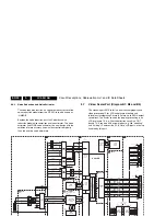
Page 85: ...dels are shown in the block diagram on the next page Figure Block diagram of the internal building blocks The architecture consists of a TV and Scaler panel an EPLD only in the Pixel Plus model an I O panel a Side I O and Local Keyboard panel and a Power Supply panel The functions for video audio processing microprocessor µP and CC Teletext TXT decoder are all combined in one IC TDA150xx item 7217...

Page 86: ...OM are supplied with 3 3 V which is also present during STANDBY The EEPROM or NVM Non Volatile Memory is used to store the settings 9 4 1 Video IF Amplifier The IF filter is integrated in a SAW Surface Acoustic Wave filter One for filtering IF video 1104 in some models 1105 and one for IF audio 1106 The type of these filters depends on the standard s that has have to be received The output of the ...

Page 87: ...H Drive Vertical East West Geometry CVBS Y VDRB H V HOUT RO GO BO INSSW3 Chroma Yint R Pr 3 G Y3 B Pb 3 YOUT VOUT UOUT VIN UIN YIN B_OSD G_OSD R_OSD Fast Blanking Peaking SCAVEM U V Delay Skin Tone U V Tint Saturation YUV YUV in out SAT SCAVEM on text Dig 2H 4H Combfilter Y Delay Adj c cvbs y Video Switch Control Uint Vint CVBS1 r AM QSS FM RO GO BO Vsync_SDTV Hsync_SDTV INTF_Y_OUT INTF_U_OUT INTF...

Page 88: ...while the other part is NTSC or SECAM In cases where a SECAM signal is presented to the Columbus Comb filter both the luminance and UV path must be bypassed The PAL delay line inside the Columbus cannot be used for SECAM signals so it must also be bypassed The luminance path must have luminance at its input instead of CVBS A chroma delay line outside Columbus must be used for SECAM signals Reason ...

Page 89: ...uminance Comb filter It tries to make an as clean as possible luminance signal out of the CVBS signal at the input The lower part receives U and V signals sequentially that are normally only band pass filtered in front of the 3D Comb filter It filters all left over luminance signals out of it in order to make an as clean as possible U and V signal The offset block receives the motion dependant 2D ...

Page 90: ...04 5 1 8 4 L4 L3 ANALOG INPUT PORT 7B010 K4D263238F SDRAM 1Mx32x4 FSDATA FSADDR 7401 GM1501 GRAPHIC ZOOM DISPLAY TIMING GEN VIDEO ZOOM OSD CONTROLLER OUT BLENDER BRIGHTNESS CONTRAST HUE SAT EXTERNAL ROM INTERFACE 7C00 MX29LV040QC FLASH ROM 512Kx8 OCMDATA OCMADDR 1P06 1 11 10 12 14 13 15 19 18 20 27 26 28 22 21 23 LVDS_VCC TXB0 TXB0 TXB1 TXB1 TXB2 TXB2 FRAME STORE CONTROL 7E02 14 2 11 15 1 12 F624 ...

Page 91: ...wo signals via the PC_HD_SEL signal and selection IC SM5301 see circuit diagram B13 PC VGA Input The VGA input is processed by the VGA block of the Scaler The Scaler supports pixel frequencies up to 165MHz 9 8 Audio Processing Figure 9 6 Block diagram audio processing The audio decoding is done entirely via the Hercules The IF output from the Tuner is fed directly to either the Video IF or the Sou...

Page 92: ...sion are used Muting is done via the SOUND_ENABLE line connected to pins 7 of both amplifier ICs which comes from the Hercules 9 8 4 Audio Lip Sync Figure 9 7 Micro Controller block diagram 9 9 3 Basic Specification The Micro Controller operates at the following supply voltages 3 3 VDC at pins 4 88 94 and 109 1 8 VDC at pins 93 96 and 117 I2 C pull up supply 3 3VDC 9 9 4 Pin Configuration and Func...

Page 93: ...This signal is used to read the status of the SCART 1 input STATUS_2 This signal is used to read the status of the SCART 2 input HERC_RESET This pin is used to switch the 1 8V supply POWER_DOWN The power supply generates this signal Logic high 3 3 V under normal operation of the TV and goes low 0 V when the Mains input voltage supply goes below 70 VAC 9 10 Abbreviation List 0 6 12 SCART switch con...

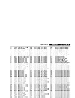
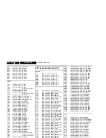
Page 94: ... Front input luminance or CVBS SVHS G SC1 IN Green SCART1 EXT1 in G SC2 IN Green SCART2 EXT2 in G TXT Green teletext H H_sync to the module HA Horizontal Acquisition horizontal sync pulse L L Monochrome TV system Sound carrier distance is 6 5 MHz L is Band I L is all bands except for Band I LS LoudSpeaker LVDS Low Voltage Differential Signalling data transmission system for high speed and low EMI ...

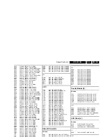
Page 95: ...ower Supply SND SouND SOPS Self Oscillating Power Supply S PDIF Sony Philips Digital InterFace This is a consumer interface used to transfer digital audio SRAM Static RAM STBY STandBY SVHS Super Video Home System SW Software or Subwoofer or Switch THD Total Harmonic Distortion TXT Teletext TXT is a digital addition to analogue TV signals that contain textual and graphical information 25 rows x 40 ...

Page 96: ...C A L B µ R E D O C E D T X E T E L E T D N A R O S S E C O R P R C B G R L B O R O G O B N I L C B N I K L B L O R T N O C B G R T R E S N I T X E T D S O C C C J D A P E T I H W N T H G I R B R T N O C X I R T A M B G R P S D o i d u a h t i w r o s s e c o r p V T o e r e t s V A e h t f o m a r g a i d k c o l B M V S s O I C Y V H O R M F O B V D H C T I W S O F E R F E R J D A Y A L E D Y M ...

Page 97: ...N C VSS SNCL TCK D E YB3 YB2 VSS VDDC TMS TDO E F TST2 YB1 VSS VSS TRST TDI F G CLKASB YB0 Do9 VDDS COLUMBUS VDDS A0ICC RESET G H CLKASA UVB8 Do8 TST3 TOP VIEW VDDC CLK EXT CLKSEL H J UVB7 Do7 UVB6 Do6 VSS VSS CLK WEN J K UVB5 Do5 UVB4 Do4 VDDC PPA Version 2 7 VSS CASN RASN K L UVB3 Do3 UVB2 Do2 VSS VDDS DQM DQ16 L M UVB1 Do1 UVB0 Do0 VDDS VSS DQ14 DQ15 M N AVD N C VDDS VSS VSS VDDC VSS VDDS VDDC ...

Page 98: ... Table RAMs Output Blender Video Shrink Filter Motion Adapt 3 2 2 2 detection Video Zoom Filter Graphics Zoom Filter Image Capture and Measure ment Internal RAM X186 Micro controller Interface Parallel ROM IF external micro Analog RGB Input Panel Data Control DDC2Bi analog DDR SDRAM I F Block Diagram Pin Configuration A NC ADC_3 3 ADC_1 8 ADC_1 8 ADC_DGND RXC DVI_GND RX0 RX1 RX2 DVI_GND LBADC_IN3 ...

Page 99: ...EEPROM Registers Configuration Logic Block XOR Mask Video Color Space Converter Up Down Sampling control signals I2C Slave 24 DE Q 23 0 DSDA DSCL R_EXT RXC RX0 RX1 RX2 INT RESET Audio Data Decode Logic Block SPDIF MCLKOUT PanelLink TMDSTM Digital Core MCLK Gen HSYNC VSYNC ODCK SD0 SCK WS MCLKIN Mode Control Aux Data Logic Block control signals Video DAC 30 AnGY AnRPr AnBPb I2 C Slave CSDA CSCL OMP...

Page 100: ...820 6 8nF 10 16V 0402 2264 3198 017 44740 470nF 10V 0603 2265 3198 017 41050 1µF 10V 0603 2266 3198 035 71040 100nF 10 16V 0402 2267 2020 552 96718 220nF 10 6 3V 0402 2269 2022 031 00373 470µF 20 16V 2270 3198 035 71040 100nF 10 16V 0402 2271 4822 124 12095 100µF 20 16V 2272 3198 035 71040 100nF 10 16V 0402 2273 2020 552 96718 220nF 10 6 3V 0402 2274 3198 017 31540 150nF 10V 0603 2277 3198 035 710...

Page 101: ...2238 869 15109 10pF 5 50V 0402 2K04 2238 869 15109 10pF 5 50V 0402 2K05 2238 869 15109 10pF 5 50V 0402 2K06 2238 869 15101 100pF 5 50V 0402 2K07 2238 869 15101 100pF 5 50V 0402 2K08 2020 552 00183 2 2µF 10 6 3V 0603 2K10 2238 869 15101 100pF 5 50V 0402 2K11 2238 869 15101 100pF 5 50V 0402 2K12 2020 552 00183 2 2µF 10 6 3V 0603 2K13 2238 869 15101 100pF 5 50V 0402 2K14 2238 869 15101 100pF 5 50V 04...

Page 102: ...3 2322 704 63302 3 3kΩ 1 0603 3734 4822 117 13602 2 2kΩ 5 0 01W 0402 3735 4822 117 13548 1kΩ 5 0402 3736 3198 031 04720 4 7kΩ 5 0402 3740 3198 031 01520 1 2kΩ 5 0 01W 0402 3741 3198 031 01520 1 2kΩ 5 0 01W 0402 3742 3198 031 01530 15kΩ 5 0 01W 0402 3743 4822 117 13601 22kΩ 5 0402 3750 4822 117 13601 22kΩ 5 0402 3751 3198 021 31080 1Ω 5 0603 3752 3198 021 31080 1Ω 5 0603 3753 2322 704 61002 1kΩ 1 3...

Page 103: ...062W 3R20 4822 051 30102 1kΩ 5 0 062W 3R22 4822 051 30759 75Ω 5 0 062W 3R23 4822 051 30101 100Ω 5 0 062W 3R28 4822 051 30759 75Ω 5 0 062W 3R29 4822 051 30101 100Ω 5 0 062W 3R35 4822 051 30101 100Ω 5 0 062W 3R36 4822 051 30103 10kΩ 5 0 062W 3R37 4822 117 12925 47kΩ 1 0 063W 0603 3R40 4822 051 30759 75Ω 5 0 062W 3R42 4822 051 30101 100Ω 5 0 062W 3R43 4822 117 12925 47kΩ 1 0 063W 0603 3R46 4822 117 1...

Page 104: ...1530 15nF 20 50V 0603 2717 2022 552 05679 1µF 10 16V 0805 2718 2222 580 15649 100nF 10 50V 0805 2719 4822 126 14583 470nF 10 16V 0805 2720 2020 021 91431 22µF 20 100V 2721 2222 580 15649 100nF 10 50V 0805 2722 4822 126 14583 470nF 10 16V 0805 2723 2022 552 05679 1µF 10 16V 0805 2726 4822 126 13193 4 7nF 10 63V 2727 4822 126 14249 560pF 10 50V 0603 2727 5322 116 80853 560pF 5 63V 2731 4822 126 1424...

Page 105: ...at 100MHz 5M11 2422 549 44197 Bead 220Ω at 100MHz 5M12 2422 549 44197 Bead 220Ω at 100MHz d 6700 4822 130 11522 UDZ15B 6702 9322 150 18685 BZX384 C47 6703 4822 130 10838 UDZ3 3B 6D10 4822 130 11397 BAS316 6D11 9340 548 69115 PDZ27B 6D12 4822 130 11397 BAS316 ce 7700 9322 202 89668 LM393P 7701 9352 729 65112 TDA8925ST N1 7702 3198 010 42310 BC847BW 7705 3198 010 42310 BC847BW 7706 3198 010 42310 BC...

Page 106: ...Revision List EN 106 LC4 9U AA 11 11 Revision List Manual xxxx xxx xxxx 0 First release Manual xxxx xxx xxxx 1 I2C Diagram positioned Spare Parts List added ...

Reviews: