background image

Mechanical Instructions

EN 9

TPM15.5L LA

4.

2015-Aug-08

back to 

div.table 

4.

Mechanical Instructions

Index of this chapter:

4.1 Cable Dressing
4.2 Service Positions
4.3 Assembly/Panel Removal
4.4 Set Re-assembly

Notes:

Figures below can deviate slightly from the actual situation, 
due to the different set executions.

4.1

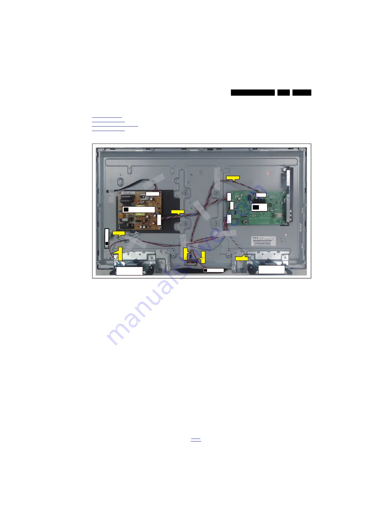
Cable Dressing

Figure 4-1 Cable dressing (32" 4900/5000 series)

19760_100.eps

CN601

CN701

CN408

CN8604

CN9101

CN401                                      

MAIN POWER SUPPLY

(1054)

A

SSB

(1053)

B

ECN408

ECN701

ECN601

ECN601

ECN401

ECN40

8

ECN401

LOUDSPEAKER

(1184)

LOUDSPEAKER

(1184)

IR/LED BOARD

(1056)

J

KEYBO

ARD CONTR

OL

(1057)

E

CN01

Summary of Contents for 32PHG4900/78

Page 1: ...ur Television Chassis TPM15 5L LA Contents Page Contents Page 1 Revision List 2 2 Technical Specs Diversity and Connections 2 3 Precautions Notes and Abbreviation List 5 4 Mechanical Instructions 9 Cable dressing 32 4900 5000 series 9 Cable dressing 40 43 5000 series 10 Cable dressing 48 5000 series 10 5 Service Modes Error Codes and Fault Finding 15 6 Alignments 23 7 Circuit Descriptions 25 8 IC ...

Page 2: ...rview Notes Figures can deviate due to the different set executions Specifications are indicative subject to change 2 1 Technical Specifications For on line product support please use the links in back to div table 2 1 Here is product information available as well as getting started user manuals frequently asked questions and software drivers Table 2 1 Described Model Numbers and Diversity 2 2 Dir...

Page 3: ...put from an antenna cable or satellite 5 Service UART 1 Ground Gnd H 2 UART_TX Transmit k 3 UART_RX Receive j 6 HDMI 2 Digital Video In Digital Audio with ARC In Out Figure 2 3 HDMI type A connector 1 D2 Data channel j 2 Shield Gnd H 3 D2 Data channel j 4 D1 Data channel j 5 Shield Gnd H 6 D1 Data channel j 7 D0 Data channel j 8 Shield Gnd H 9 D0 Data channel j 10 CLK Data channel j 11 Shield Gnd ...

Page 4: ... D1 Data channel j 7 D0 Data channel j 8 Shield Gnd H 9 D0 Data channel j 10 CLK Data channel j 11 Shield Gnd H 12 CLK Data channel j 13 Easylink CEC Control channel jk 14 ARC Audio Return Channel k 15 DDC_SCL DDC clock j 16 DDC_SDA DDC data jk 17 Ground Gnd H 18 5V j 19 HPD Hot Plug Detect j 20 Ground Gnd H 8 Cinch Digital Audio Out BK Coaxial 0 4 0 6VPP 75 W kq 2 4 Chassis Overview Refer to 9 Bl...

Page 5: ...the power supply section both in normal operation G and in stand by F These values are indicated by means of the appropriate symbols 3 3 2 Schematic Notes All resistor values are in ohms and the value multiplier is often used to indicate the decimal point location e g 2K2 indicates 2 2 k Resistor values with no multiplier may be indicated with either an E or an R e g 220E or 220R indicates 220 All...

Page 6: ...tion It is easy to do and is a good service precaution 3 4 Abbreviation List 0 6 12 SCART switch control signal on A V board 0 loop through AUX to TV 6 play 16 9 format 12 play 4 3 format AARA Automatic Aspect Ratio Adaptation algorithm that adapts aspect ratio to remove horizontal black bars keeps the original aspect ratio ACI Automatic Channel Installation algorithm that installs TV channels dir...

Page 7: ...sed for broadcast grade video Uncompressed digital component or digital composite signals can be used The SDI signal is self synchronizing uses 8 bit or 10 bit data words and has a maximum data rate of 270 Mbit s with a minimum bandwidth of 135 MHz iTV Institutional TeleVision TV sets for hotels hospitals etc LS Last Status The settings last chosen by the customer and read and stored in RAM or in ...

Page 8: ...SD Standard Definition SDA Serial Data I2C SDA F DAta Signal on Fast I2C bus SDI Serial Digital Interface see ITU 656 SDRAM Synchronous DRAM SECAM SEequence Couleur Avec Mémoire Colour system mainly used in France and East Europe Colour carriers 4 406250 MHz and 4 250000 MHz SIF Sound Intermediate Frequency SMPS Switched Mode Power Supply SoC System on Chip SOG Sync On Green SOPS Self Oscillating ...

Page 9: ...Re assembly Notes Figures below can deviate slightly from the actual situation due to the different set executions 4 1 Cable Dressing Figure 4 1 Cable dressing 32 4900 5000 series 19760_100 eps CN601 CN701 CN408 CN8604 CN9101 CN401 MAIN POWER SUPPLY 1054 A SSB 1053 B ECN408 ECN701 ECN601 ECN601 ECN401 ECN408 ECN401 LOUDSPEAKER 1184 LOUDSPEAKER 1184 IR LED BOARD 1056 J KEYBOARD CONTROL 1057 E CN01 ...

Page 10: ...CN9101 CN403 MAIN POWER SUPPLY 1054 A SSB 1053 B ECN408 ECN701 ECN601 ECN601 ECN403 ECN408 ECN403 LOUDSPEAKER 1184 LOUDSPEAKER 1184 IR LED BOARD 1056 J KEYBOARD CONTROL 1057 E CN01 19760_102 eps CN601 CN701 CN403 CN408 CN8101 CN9301 MAIN POWER SUPPLY 1054 A SSB 1053 B ECN408 ECN701 ECN601 ECN601 ECN403 ECN408 ECN403 LOUDSPEAKER 1184 LOUDSPEAKER 1184 IR LED BOARD 1056 J KEYBOARD CONTROL 1057 E CN01...

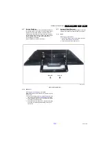
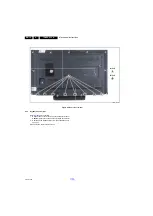
Page 11: ...0 78 but will be similar for other 5000 series and 32 4900 series models 4 3 1 Stand Refer to Figure 4 4 for details 1 Remove the fixation screws 1 that secure the stand bracket Refer to Figure 4 4 for details 2 Take the stand bracket out from the set Figure 4 4 Stand removal 4 3 2 Rear Cover Refer to Figure 4 4 and Figure 4 5 for details Warning Disconnect the mains power cord before removing the...

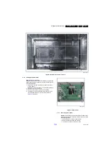
Page 12: ... Control Unit Refer to Figure 4 6 for details 1 Release the connector 2 from the keyboard control panel Caution be careful as these are very fragile connectors 2 Remove all the fixation screws from the keyboard control panel 1 When defective replace the whole unit 19760_103 eps 2 2 2 2 2 2 2 2 2 2 2 2 3 M3 8 2 M3 6 3 4 ...

Page 13: ... these are very fragile connectors 2 Unplug all other connectors 2 3 Remove all the fixation screws from the SSB 3 4 The SSB can now be shifted from side connector cover then lifted and taken out of the I O bracket Refer to Figure 4 7 for details Figure 4 7 SSB removal 4 3 5 Power Supply Unit PSU Caution it is mandatory to remount all different screws at their original position during re assembly ...

Page 14: ...Remove the PSU as described earlier 3 Remove the keyboard control panel as described earlier 4 Remove the stand bracket as described earlier 5 Remove the IR LED as described earlier 6 Remove the fixations screws that fix the metal clamps to the front bezel Take out those clamps 7 Remove all other metal parts not belonging to the panel 8 Lift the LCD Panel from the bezel When defective replace the ...

Page 15: ...r is kept called Op Hour It counts the normal operation hours not the Stand by hours The actual value of the timer is displayed in SAM in a decimal value Every two soft resets increase the hour by 1 Stand by hours are not counted Software Identification Version and Cluster The software ID version and cluster will be shown in the main menu display of SAM and CSM The screen will show AAAAB X YYY whe...

Page 16: ...wing key sequence on the remote control transmitter from the menu home press 1999 directly followed by the Back Return button Do not allow the display to time out between entries while keying the sequence After entering the Factory mode the following items are displayed Main Menu Sub menu 1 Sub menu 2 Description System Information Op Hour e g 00057 This represents the life timer The timer counts ...

Page 17: ...ss is displayed remove the power and restart the TV 9 CLR_TEMP_R 128 128 128 128 Red colour temperature setting 10 CLR_TEMP_G 125 128 128 128 Green colour temperature setting 11 CLR_TEMP_B 102 128 128 128 Blue colour temperature setting 12 AUTO_COLOR Press OK PC any pattern that has black and white YPbPr SMPTE bar colour bar any timing 13 ADC_GAIN_R 0 Red ADC gain 14 ADC_GAIN_G 128 128 128 128 Gre...

Page 18: ...ion number has to be re written to NVM This identification number is the 12NC number of the SSB 1 6 Display 12NC NVM read write 1 7 PSU 12NC NVM read write 2 1 Current Main SW Displays the built in main software version In case of field problems related to software software can be upgraded As this software is consumer upgradeable it will also be published on the internet 2 2 Standby SW Displays th...

Page 19: ...s Power Plug Standby Soft Mode Command Received previously in Standby Soft Mode Power tact switch TV Wakeup commands Received TV Wakeup keys Digital background tasks started Digital background tasks completed Swith On previously in Standby Semi Standby Mains Power Plug Standby Soft Mode Command Received Power tact switch Switch Off Mains Power Plug Switch Off Mains Power Plug Swith On previously i...

Page 20: ...ts products and it s recommend that the TV software is updated when updates are available Software update files can be obtained from the dealer or can be downloaded from the following websites http www philips com support Preparing a portable memory for software upgrade The following requirements have to be met 1 A personal computer connected to the internet 2 An archive utility that supports the ...

Page 21: ...or every Activated SW protection Failing I2C device General I2 C error The last five errors stored in the NVM are shown in the Service menu s This is called the error buffer The error code buffer contains all errors detected since the last time the buffer was erased The buffer is written from left to right When an error occurs that is not yet in the error code buffer it is displayed at the left si...

Page 22: ...single bytes can be changed Caution Do not change these without understanding the function of each setting because incorrect NVM settings may seriously hamper the correct functioning of the TV set Always write down the existing NVM settings before changing the settings This will enable you to return to the original settings if the new settings turn out to be incorrect 5 8 2 Load Default NVM Values...

Page 23: ...er e g Minolta CA 210 in the centre of the screen Consequently the measurement needs to be done in a dark environment Adjust the correct x y coordinates while holding one of the White point registers R G or B on max value by means of decreasing the value of one or two other white points to the correct x y coordinates see Table 6 1 White D alignment values Tolerance dx 0 003 dy 0 003 Repeat this st...

Page 24: ... The loading of the CTN and production code can also be done via ComPair Model number programming In case of a display replacement reset the Operation hours display to 0 or to the operation hours of the replacement display Remark After the NVM has been replaced go to SAM and scroll to the Reload MAC address see figure 1 Select the item and press OK on the RC 6 5 1 Reset of Repaired SSB Instruction...

Page 25: ... Circuit Diagrams and PWB Layouts Where necessary you will find a separate drawing for clarification 7 1 Introduction The TPM15 5L LA is a new chassis launched in LATAM in 2015 The whole range is covered by MT5561 The major deltas versus its predecessor support NTSC PAL M PAL N AND ISDB T with also multi media CEC ARC SPDIF functionality The TPM15 5L LA chassis comes with the following stylings se...

Page 26: ...ptions EN 26 TPM15 5L LA 7 2015 Aug 08 back to div table 7 1 3 SSB Cell Layout Figure 7 1 SSB layout cells top view 19760_200 eps USB Headphone SERVICE CONNECTOR HDMI HDMI ANALOG I O MT5561 TUNER DDR DC DC SPDIF OUT ...

Page 27: ...power on mode 12V bolt on power on mode 22V bolt on power on mode Stand by mode for 40PFG5000 78 16V bolt on power on mode Stand by mode for 32PHG5000 78 Output to the display in case of IPB High voltage to the LCD panel PSL and PSLS LED driver outputs PSDL high frequent AC current 7 2 2 Diversity The diversity in power supply units is mainly determined by the diversity in displays The following d...

Page 28: ...graphical representation of the DC DC converters with its current consumptions Number Connector 32 40 43 48 CN9101 CN8604 CN9101 CN8601 CN9301 CN8101 Description to SSB to Panel to SSB to panel to SSB to panel Pin 14 6 16 12 14 12 1 DIM VLED DIM VLED DIM VLED 2 On off VLED On off n c On off n c 3 PS_ON n c PS_ON VLED PS_ON VLED_1 4 Scan_BL_EN n c n c VLED 2D 3D VLED_1 5 GND LED_a GND n c GND n c 6...

Page 29: ... detection TMDS output control CEC control 7 6 Video and Audio Processing MT5561LVNT B PBGA 329 The MT5561LVNT B is the main audio and video processor or System on Chip for this platform It has the following features Multi standard digital video decoder MPEG 1 2 H 264 MPEG 4 A transport de multiplexer A muti standard video decoder Rich format audio codec HDMI 1 4a receiver with 3D support 2D 3D co...

Page 30: ...TSC PAL SECAM ATD TV Decoder TS Demux Video ADC Video Input De interlace HDMI Rx Audio Input Audio Demod Audio ADC SPDIF In Grapihc DDR3 Controller OSD scaler Audio DSP Audio I F Audio DAC JTAG IrDA PCR I2 C RTC UART SDIO USB2 0 PWM Ethernet Watchdog Serial Flash NAND Flash Servo ADC SPDIF Out I2 S ADAC L R x 2 TS Input Tuner Input CVBS YC Input Component Analog Input SIF Audio Input Panel 16 bit ...

Page 31: ...DD7 POCE0 POWE PDD5 DVSS VCCK DVSS K K PACLE PAALE PDD2 PARB VCCK VCCK VCCK VCCK DVSS DVSS L L VCCK VCCK VCCK VCCK VCCK VCCK VCCK VCCK DVSS DVSS M M DVSS DVSS DVSS DVSS DVSS DVSS VCCK VCCK DVSS DVSS N N DDRV DDRV DDRV DDRV DDRV DDRV DVSS DVSS DVSS VCC3IO P P DDRV REF ZQ AOLRC K OSDA0 DVSS ADIN1 VCC3IO VCC3IO R R AOBC K AOMCLK AOSDAT A0 ASPDIF O OSCL0 DVSS ADIN7 AVDD33_E TH AVDD33_HD MI T T OPWRSB ...

Page 32: ...DVSS DVSS HDMI_2_SDA IF_AGC HDMI_2_HPD_CBUS HDMI_2_SCL HDMI_1_SCL HDMI_2_RX_2 HDMI_2_RX_2B K K DVSS DVSS HDMI_1_SDA MHL_SENCE HDMI_CEC HDMI_2_RX_0 HDMI_2_RX_1 HDMI_2_RX_1B L L DVSS DVSS DVSS AVDD33_CAP RF_AGC HDMI_1_HPD HDMI_2_RX_0B M M DVSS DVSS DVSS AVDD33_AADC AVDD33_ADAC HDMI_2_RX_C HDMI_2_RX_CB HDMI_1_RX_2 HDMI_1_RX_2B N N DVSS DVSS DVSS AVSS33_CLN DVSS DVSS HDMI_1_RX_1 HDMI_1_RX_1B P P DVSS ...

Page 33: ...1 AGND AGND LX PGND IN1 OUT2 M5723B 9 6 5 EN2 IN2 Thermal Pad IN1 CONTROL HDRV A1 100mΩ 80mΩ LDRV R S Q Thermal Shutdown UVLO OSC Compensation EA VREF LX Zero Current Detect Current Sense OC 0 6V FB1 IN2 OUT2 SHUTDOWN LOGIC 1 25V Vref 炼 ERROR AMP 為 OVER CURRENT PROTECT DYNAMIC FEEDBACK AGND R1 R2 OVER TEMP PROTECT EN1 PGND EN2 IN1 CONTROL HDRV A1 100mΩ 80mΩ LDRV R S Q Thermal Shutdown UVLO OSC Com...

Page 34: ...BSTRPD PVDD GVDD_REG DR_SDI SSTIMER ANA_REG2 AGND DGND DVDD TEST3 RST NC SCL SDA SDIN SCLK LRCLK PDN Digital Audio Processor Clock Monitoring Open Loop Digital PWM Modulator Full Bridge Power Stage B Serial Audio Port Internal Control Registers and State Machines Over Current Protection Full Bridge Power Stage A Gate Drives Gate Drives Die Temp Monitor PWM Power Stage SPK_OUTC SPK_OUTD SPK_OUTA SP...

Page 35: ...2 21 20 19 18 17 16 15 14 13 7 8 9 10 11 12 1 2 3 4 5 6 LNA_INP LNA_INN AS GND_XTAL CLK_OUT XTAL_P XTAL_N VDD_1p8 VDD_IO AGC_1 AGC_2 GPO_3 MxL661 VDD_3p3 RESET_N VDD_1p8 VDD_1p8 GND_DIG VDD_1p2 IF_OUTN_1 IF_OUTP_1 IF_OUTP_2 GPO_1 IF_OUTN_2 GPO_2 SDA SCL VDD_3p3 Crystal Reference I2 C Voltage Regulator AGC1 RF Synth Gain Control IF Synth Synth Calibration LNA AGC2 Channel Filtering CLK_OUT IF1 Out ...

Page 36: ... VREFH G F 7 3 5 0 9 C T Synchroni za tion flag TS output Crystal reference clock Tuner AGC control IIC control Filter AGC ISIC unguarded pre post echo suppression FFT Control Adaptive interpolation filter Equalization With Doppler Com pensation CSI Reliability detection CVI CW interference detection AGC control output Tuner IIC Clock PLL Viterbi decoding Memory Frequency deinterleaving RS decodin...

Page 37: ...19760_400 eps 5W SPK L CVBS L R AUDIO AMP KeyPad Silicon Tuner MxL661 AG R HDMI1 Headphone AMP L R MT5561 ATV LVDS UART CN103 Side IF HDMI2 w ARC USB2 CN501 Side TI 31100 R PC Audio in Headphone APA2176A CN502 Rear USB1 Share to Wi Fi modul Remote Control 5W SPK L R VGA SPIDF Out CN104 Rear DTV DEMOD TC90537 TSB Demod ...

Page 38: ...K 1 8W 5 C9120 100P 50V C9120 100P 50V R8610 0 2oHM 1 1 4W R8610 0 2oHM 1 1 4W R9127 NC 100K 1 8W 1 R9127 NC 100K 1 8W 1 JR901 0R05 1 4W JR901 0R05 1 4W D9106 1N4007 D9106 1N4007 C8612 100N 50V C8612 100N 50V R9129 30 OHM 1 4W FB9905 BEAD FB9905 BEAD 1 2 T9101 POWER X FMR T9101 POWER X FMR 1 2 4 5 6 7 11 10 8 C9902 NC 470NF 305V C9902 NC 470NF 305V C9104 100N 50V C9104 100N 50V C9117 470UF 25V C91...

Page 39: ...C9801 C8608 C9106 C9111 C9103 D9101 F9901 J905 J901 J909 J911 J906 J904 J902 J914 C8615 J908 J910 J912 J913 J903 R9101 T9101 D8601 S6 S7 S3 S4 S5 S8 S9 S10 S11 S12 S13 S15 C9102 C9117 C9118 C9901 C9905 C9903 C9904 CN8601 CN8602 D9105 FB9901 HS9101 L9101 MH5 MH1 MH4 Q9102 C8601 C9115 FB9905 MH3 MH2 FB9906 C9902 L8601 ZD9102 L8602 Q9101 RV9901 CN9101 C9906 C9907 FB9907 FB9908 GND3 L9901 L9902 NR9901...

Page 40: ...SM6 SM7 R9115 Q8601 IC8601 R9139 R9140 R9141 R9142 C8603 Q8603 IC9103 C8611 C8610 C8612 C8607 C8606 C9107 C9108 C9109 C8609 D9103 R8609 R8605 R8607 R8603 R8604 R8613 R8612 R8606 R8610 R8608 R8614 R8615 R8616 R9102 R9104 R9106 R9107 R9109 R9103 R9110 R9127 R9128 R9129 R9901 R9902 R9903 R9904 R9905 R9906 JR901 JR902 R8611 SM5 C8613 R8602 R9108 C8614 C8605 R8601 R9105 R9121 R9122 R9123 R9124 R9125 R9...

Page 41: ...OHM 1 8W U9102 EL817M X 1 2 3 4 C9111 100N 50V R9112 3 3M 1 4W R9111 2M2 5 1 2W R9103 10 OHM 1 4W R9113 3 3M 1 4W R9173 680R 1 8W 1 R9114 3 3M 1 4W HOT COLD D9102 SS1060FL R9102 47K 1 4W R9163 33ohm 1 4W 5 R9162 33ohm 1 4W 5 R9161 33ohm 1 4W 5 C9801 82UF 450V R9105 75K FB_1 R9171 2K OHM 12V1 C9152 470UF 25V L9101 3UH R9121 150 OHM 1 4W R9122 150 OHM 1 4W R9123 150 OHM 1 4W 12V1 GND1 GND 1 C9912 10...

Page 42: ...50V R8604 NC R8616 1R2 1 R8608 10K 1 8W R8607 5 1R 1 8W C8601 220uF 50V FB8601 BEAD 1 2 R8614 1R2 1 C8606 1uF R8609 10R 1 8W 5 22V ON OFF OUT DIM OUT VLED VLED R8618 1R2 1 ZD8602 NC BZT52 B22 1 2 FB8602 NC BEAD 1 2 R8622 10K 1 8W 1 C8615 100N 50V Q8602 LMBT3906LT1G R8620 2K2 1 8W C8617 100N 50V C8614 NC 22UF 50V D8605 NC 1N4148 R8621 1K 1 8W 1 12V R8602 NC 0R05 1 4W CN8601 CONN 1 2 3 4 5 6 7 8 9 1...

Page 43: ... J925 T9101 D8601 D8602 D8605 J926 H3 H4 H5 H6 TP2 TP3 TP4 TP5 TP6 TP7 TP9 TP8 DR1 MH2 MH1 MH7 MH8 MH6 MH5 MH4 MH3 C8603C8604 C9907 C9104 C9105 C9112 C9151 C9152 C9153 C9154 C9160 C9121 C9122 C8601 C9302 C9306 C9912 C9911 C9913 C9914 C9921 C9920 CN9902 D9151 D9121 FB9301 FB8601 GND1 GND2 GND3 HS9101 HS9151 HS9121 L8601 L8602 L9101 L9301 L9901 L9902 Q9121 R9907 SG9901 SG9902 HS9901 FB9904 FB9902 HS...

Page 44: ...5 R8616 R8617 R9102 R9104 R9106 R9107 R9109 R9103 R9110 R9172 R9174 R9161 R9162 R9163 R9164 R9173 R9171 R9175 R9176 R9181 R9182 R9183 R9184 R9186 R9127 R9128 R9129 R9301 R9302 R9303 R9304 R9305 R9306 R9901 R9902 R9903 R9904 R9905 R9906 U9101 U8601 U9301 R9185 U9901 JR901 JR902 SM2 SM3 SM4 R8611 SM5 C9301 C8613 R8602 R8618 R8619 JR903 R9108 JR904 C9156 C9157 C8615 C8616 C8617 R8620 R8621 R8622 R862...

Page 45: ...F 250V C9904 100PF 250V 1 2 HS9902 HEAT SINK SG9901 NC SG9902 NC RV9901 680V 1 2 CN9901 SOCKET COLD HOT R9901 NC R9903 NC 1 2 3 4 HS9901 HEAT SINK C9902 100NF 305V 1 2 4 3 L9902 12mH C9901 100NF 305V 1 2 3 4 F9901 FUSE 1 2 t NR9901 2 5R C9907 470pF 250V C9908 NC 1 2 4 3 L9901 12mH 1 2 t NR9902 2 5R B Vsin A A B 2 1 3 4 BD9901 TS10K80 02 NC 1 D1 2 D1 3 NC 4 NC 5 D2 6 D2 7 NC 8 IC9901 NC C9906 470pF...

Page 46: ... 8W 1 C8144 100N 50V R8136 20K OHM Q8147 P5002CMG 1 GND806 GND 1 GND807 GND DIM 1 GND801 GND 1 2 3 4 HS8101 HEAT SINK R8147 0R68 1W 5 R8146 0R68 1W 5 1 GND804 GND 1 GND802 GND C8131 1N 50V 1 GND805 GND R8115 1M 1 8W 5 C8106 100N 50V R8156 0R68 1W 5 Q8143 MTBA5N10J3 Q8145 P5002CMG R8157 0R68 1W 5 R8109 100KOHM 1 1 8W R8110 240K 1 1 8W Q8149 MTBA5N10J3 R8164 200K OHM G2 SENSE2 1 2 FB8101 127R VLED_1...

Page 47: ...NF R9121 12K 5 1 4W R9105 0 1R B VCC 1 VREF 3 G 4 OV UV 5 FB 6 DT BF 7 IS 8 NC 9 S1 10 S2 11 HB 13 VCCH 14 D 16 IC9101 LCS700LG TL R9101 1MOHM 1 1 4W R9124 2 4KOHM 1 1 8W R9114 22KOHM 1 1 8W R9102 1MOHM 5 1 2W R9103 1MOHM 5 1 2W R9127 43R 1 C9127 1uF C9128 1uF 1 2 3 D9104 FMEN 2308 C9117 2 2nF 50V D9106 SS1060FL C9126 2 2nF 50V 36V 24V R9110 8 2K 1 4W C9116 47nF 50V R9109 120R 1 R9111 150KOHM 1 1 ...

Page 48: ...1 1 8W R9315 470 OHM 1 4W R9336 2Kohm 1 4W 5 R9316 2 2 OHM 1 4W R9314 0 27R R9308 100K 1 4W R9347 2 2KOHM 1 1 8W C9332 10UF 50V R9338 100K 1 8W 1 R9312 51 OHM 1 4W R9335 10K OHM 5 1 8W R9332 330K 1 1 8W 1 2 4 3 IC9331 PS2561DL1 1 C9304 1N 50V R9341 10K OHM 5 1 8W Q9331 2N7002K R9301 6 8K 1 4W C9301 10NF C9315 100N 50V C9312 470UF 25V R9309 100K 1 4W R9310 100K 1 4W C9341 220N 50V 1 2 ZD9330 BZT52 ...

Page 49: ...91T C9813 1UF 450V Q9801 TK16A60W VCC_ON HOT COLD D9802 MUR460 28 1 2 L9803 NC C9814 470pF 250V R9807 10 OHM 1 8W R9808 75 OHM 1 8W C9807 1N 50V 1 2 3 4 HS9801 HEAT SINK R9813 10K 1 8W R9810 470 OHM 1 4W R9805 20K 1 4W R9811 0 1R C9801 1UF 450V D9806 NC FMNS 1106S 3 1 4 5 L9801 240UH R9814 NC C9809 100P 50V 1 2 FB9802 BEAD R9812 27K 1 8W 1 C9806 470NF 50V R9806 3 3KOHM 1 1 8W C9810 68uF 450V C9811...

Page 50: ...SU4 SU1 J9147 J9101 SU3 R8144 R8145 R8146 R8147 R8156 R8157 HS1 HS2 HS3 H5 H10 H8 H7 H6 H9 H2 MH12 H11 GND1 BD9901 C8101 C9101 C9106 C9121 C9122 C9123 C9301 C9306 C9311 C9312 C9313 C9314 C9317 C9318 C9810 C9811 C9812 C9907 C9908 CN8101 CN9901 D8101 D9104 D9305 D9306 F9901 FB9101 FB9802 HS9101 HS9301 HS9801 HS9901 IC9101 L8101 L9102 L9301 L9801 L9901 L9902 NR9901 NR9902 Q9301 Q9801 R9811 R9901 R990...

Page 51: ...9127 R9137 R9139 R9140 R9301 R9302 R9303 R9305 R9307 R9308 R9309 R9310 R9311 R9312 R9313 R9315 R9316 R9318 R9319 R9320 R9321 R9324 R9325 R9332 R9333 R9334 R9336 R9337 R9338 R9341 R9344 R9345 R9347 R9348 R9801 R9802 R9803 R9804 R9805 R9806 R9807 R9808 R9809 R9810 R9812 R9813 R9814 JR8105 R9342 R8143 SE7 SE5 SE6 R9114 R9128 R9115 R9343 Q8145 Q8147 R8120 R8123 R9124 R9322 R9323 R9815 IC9801 IC9901 R8...

Page 52: ...3 14 DVDD3V3 Q703 LMBT3904LT1G AVDD1V2 8 13 15 5VSB Q702 NC SM4310PSKC S 1 S 2 S 3 G 4 D 8 D 7 D 6 D 5 OPWRSB 4 INVERTER_ON_OFF BL_ON OFF Q707 MMBT3904 BL_DIMMING 14 3V3SB BL_DIMMING BRIGHT ADJUST Max 3 3V Min 0V U703 M5723B 33F61U EN1 1 IN1 8 AGND 2 LX 10 AGND 4 EN2 5 FB1 3 OUT2 7 IN2 6 PGND 9 tGND 11 R780 4 7K 1 16W C706 1UF 10V C708 NC 4 7UF 10 10V R706 100K 1 Q704 LMBT3906LT1G R749 36K 1 R754 ...

Page 53: ... E2 3 VSS 4 SDA 5 SCL 6 WC 7 VCC 8 PAALE TP401 FSRC_WR STRAPPING OSCL0 OSDA0 U0RX U0TX SYS_EEPROM_WP U405 TC58NVG0S3ETAI0 CLE 16 I O0 29 R B1 7 VSS 13 VDD 12 VDD 37 VSS 36 ALE 17 I O1 30 I O2 31 I O3 32 I O4 41 I O5 42 I O6 43 I O7 44 NC 1 NC 2 NC 3 NC 4 NC 5 NC 6 NC 10 NC 11 NC 14 NC 15 NC 20 NC 21 NC 22 NC 23 NC 24 NC 25 NC 26 NC 27 NC 28 NC 33 NC 34 NC 35 NC 38 NC 39 NC 40 NC 45 NC 46 NC 47 NC ...

Page 54: ...Normal MCLK C660 6 8NF 50V C661 6 8NF 50V SPDIF_OUT SPDIF_OUT 9 R625 10 OHM 1 10W CVBS_L_IN 8 CVBS_R_IN 8 CVBS_R_IN CVBS_L_IN R626 10 OHM 1 10W AL0O AR0O HPR_IN HPL_IN HPR_IN 6 HPL_IN 6 A B CN605 NC CONN 2 1 4 3 AR0O U401C MT5561LVNT AIN_L0 U20 AIN_L1 V20 AIN_L2 T20 AIN_L3 T19 AIN_R0 R20 AIN_R1 R17 AIN_R2 R19 AIN_R3 R18 AL0_ADAC R16 AR0_ADAC P16 AL1_ADAC T18 AR1_ADAC U19 ASPDIFI F16 ASPDIFO R4 AOM...

Page 55: ...4 OUTC 45 BSTC 46 BSTB 47 OUTB 48 GND 36 GND 35 TEST 33 DVDD 34 RESET 32 NC 31 SCL 30 SDA 29 SDIN1 28 SCLK 27 LRCLK 26 PDN 25 CP 13 HPVDD 14 GND 15 FLTM 16 FTLP 17 AVDD_REG1 18 AVDD 19 ADR 20 MCLK 21 ROSC 22 GND 23 DVDD_REG 24 E Pad 49 C637 47nF 16V C615 10UF 6 3V 20 C610 10UF 6 3V 20 FB603 120R 1 2 C633 2 2nF 50V R613 10K 1 1 16W C628 33nF50V R611 1K 1 16W 1 C642 4 7UF 10 10V C612 100NF 16V C613 ...

Page 56: ...BS3P 8 OSDA2 12 14 IF_AGC 12 14 AVDD1V2 2 9 12 13 14 SOY0 8 AVDD3V3 2 4 5 9 10 11 12 13 ARC 13 Analog Power AVDD12_DEMOD AVDD12_RGB AVDD33_DEMOD AVDD33_VIDEO AVDD1V2 SPDIF_OUT YPbPrL_IN Y_IN_1 YPbPrR_IN SPDIFOUT PB_IN_1 YPbPr Audio IN PR_IN_1 IF_AGC YPbPrL_IN YPBPR0_L_IN YPBPR0_R_IN YPbPrR_IN IF_AGC PB1P TU_FAT_IN2 AVDD3V3 PR_IN_1 PB_IN_1 YPBPR IN PR1 PB1P COM1 PR1P SOY1 Y1P Y1 PB1 Y_IN_1 CVBS1P V...

Page 57: ...3 01H 1 2 ZD102 NC AZ5123 01H 1 2 ZD103 NC AZ5123 01H 1 2 ZD104 NC AZ5123 01H 1 2 YPbPr Video Audio Input U401D MT5561LVNT VGA_SCL V5 VGA_SDA V4 VSYNC V10 HSYNC U10 BP V11 SOG U11 GP W12 COM Y12 RP V12 SOY1 U12 Y1 V13 COM1 U13 PB1 W14 PR1 Y14 SOY0 V14 Y0 U14 COM0 V15 PB0 U15 PR0 W16 VDAC_OUT W17 CVBS1 Y17 CVBS0 V18 ADCINP_DEMOD W18 ADCINN_DEMOD Y19 AVDD33_RGB_STB V17 AVDD33_VIDEO_STB U17 AVDD12_DE...

Page 58: ...V 20 Q601 LMBT3904LT1G R669 10K 1 1 16W DVDD3V3 DVDD3V3 5V_SW DVDD3V3 3 4 5 6 8 10 11 13 15 16 17 18 5VSB DVDD3V3 5V_SW 3 10 11 12 15 HP_AC_MUTE 6 HP_MUTE 10 5VSB 3 7 16 GND 3 4 5 6 7 8 10 11 12 13 14 15 16 17 18 5VSB 5V_SW C677 NC 100N 16V R656 NC 33R 1 16W 5 CN603 NC CONNNECTOR GND 1 VCC 2 VIN 3 5V_SW SPDIF_OUT 5 15mil SPDIF_OUT R624 100R 1 16W 5 C685 100NF 16V R654 180R 1 16W 5 CN604 RCA JACK 1...

Page 59: ... A2 AO0N B2 TCON0 E4 TCON1 F2 TCON2 C2 TCON3 E3 TCON4 C1 TCON5 D1 TCON6 F3 TCON7 D2 TCON8 F1 C476 NC 10N 50V U403 NC SY8104ADC LX 5 FB 1 EN 2 GND 3 IN 4 BS 6 C479 NC 22UF 10V R488 0R051 8W R484 NC 10K 1 10W 1 C478 NC 22UF 10V AC_Off Q422 NC BC847C 3V3SB LED_PWR_Blue L402 NC 4 7uH R4052 NC 1 2K 1 16W R485 NC 36K 1 R487 NC 40 2K 1 16W 1 R486 NC 20K OHM 1 16W 1 LED B LED R R483 NC 191K OHM 1 1 16W R4...

Page 60: ...V 20 R133 560R 1 16W 1 C134 1nF 50V C190 1UF 10 16V Control Interface IF Interface R156 330R 1 16W 1 FB108 1000R 1 2 Notch_On1 C133 10UF 6 3V 20 TUNER_SCL TUNER_SDA IFAGC_Toshiba_demo FCN101 RF CONN 1 1 2 2 3 3 4 4 ANT 5 SW_CTL 10 SW_CTL R149 1K 1 16W 1 C143 10N 50V IFAGC_Toshiba_demo T_SCL T_SDA TUNER_SDA TUNER_SCL R116 0R05 1 10W ADCINP_DEMOD 8 ADCINN_DEMOD 8 TUNER3 3V FAT_IN FAT_IN R127 1K 1 16...

Page 61: ...V C430 10UF 6 3V 20 L401 2 2uH C196 NC 4 7UF 10 10V RVREF Main Chip Ref Voltage C436 100NF 16V U401A MT5561LVNT DDRV N1 DDRV N2 DDRV N3 DDRV N4 DDRV N5 DDRV N6 DDRVREF P1 ZQ P2 TN_MEMPLL H8 TP_MEMPLL J8 RVREF R410 100K 1 ZQ R2 DRAM POWER DDRV R1 5V_SW R461 1K 1 16W 1 C433 100NF 16V C429 NC 100N 16V C438 100NF 16V C440 4 7UF 10 10V R455 1K 1 16W 1 R457 240R 1 C434 100NF 16V C432 100NF 16V C425 NC 1...

Page 62: ...2B W9 HDMI_0_RX_2 Y9 HDMI_0_SCL U7 HDMI_0_SDA V6 HDMI_0_HPD W5 AVDD33_HDMI R10 AVDD12_HDMI_0 Y5 HDMI_1_RX_CB P20 HDMI_1_RX_C P19 HDMI_1_RX_0B P18 HDMI_1_RX_0 P17 HDMI_1_RX_1B N18 HDMI_1_RX_1 N17 HDMI_1_RX_2B M20 HDMI_1_RX_2 M19 HDMI_2_RX_CB M18 HDMI_2_RX_C M17 HDMI_2_RX_0B L18 HDMI_2_RX_0 K18 HDMI_2_RX_1B K20 HDMI_2_RX_1 K19 HDMI_2_RX_2B J20 HDMI_2_RX_2 J19 HDMI_CEC K16 HDMI_2_SCL J17 HDMI_2_SDA J...

Page 63: ...TRL2 V3 OPCTRL3 V1 OPCTRL4 U4 ADIN7 R8 ADIN6 T6 ADIN5 U5 ADIN4 T8 ADIN3 U6 ADIN2 U8 ADIN1 P8 ADIN0 T7 GPIO2 G17 GPIO3 H5 GPIO4 H4 GPIO5 F17 OPCTRL0 U3 USB_PWR_EN0 LED_PWR_GREEN LVDS_PWR_EN BL_ON OFF BL_DIMMING USB_PWR_EN0 SYS_EEPROM_WP KEY_UP_DN_DCSW KEY_MENU_L_R_SOURCE USB_PWR_OCP0 GND 3 4 5 6 7 8 9 10 11 12 13 15 16 17 18 AMP_MUTE AMP_MUTE 6 AMP_MUTE BL_DIMMING WiFi_PWR_EN WiFi_PWR_EN 15 KEY_MEN...

Page 64: ...7 D12 CI_MCLKO A12 CI_RESET C12 CI_A6 B12 CI_A5 E10 CI_WAIT C11 CI_A4 D10 CI_A3 A10 CI_REG B10 CI_MOVAL C10 CI_A2 F10 CI_MOSTRT D11 CI_MDO0 E11 CI_A0 D9 CI_MDO1 E7 CI_MDO2 E8 CI_PWR_EN F18 CI_D0 B8 CI_D1 D13 CI_D2 F9 CI_CD2 F7 U401F MT5561LVNT USB_DM0 H19 USB_DP0 H18 USB_DM1 G19 USB_DP1 F19 RXVN W2 RXVP W3 TXVN Y1 TXVP Y2 AVDD33_ETH R9 AVDD12_ETH Y4 REXT_ETH W4 AVDD1V2 3 8 13 AVDD1V2 TP410 TP411 T...

Page 65: ...ble control H OFF state Debug mode HDMI pin14 12V ARC_SPDIF R467 40 2K 1 16W 1 U0TX U0RX R466 60 4K 1 R464 10K 1 1 16W 5VSB HDMI_SCL2 HDMI_SDA2 Q404 LMBT3904LT1G ARC_SPDIF UART_SEL HDMI_SDA2 TX HDMI_SCL2 RX HDMI_SDA2 HDMI_SDA2 TX HDMI_SCL2 RX HDMI_SCL2 R493 NC 0R05 1 16W R494 NC 0R05 1 16W U410 74CBTLV1G125GW OE 1 A 2 GND 3 B 4 Vcc 5 R468 10K 1 1 16W R470 180R 1 10W 1 C444 1UF 25V R471 82R 1 10W 1...

Page 66: ...1J MT5561LVNT VCCK K6 VCCK K5 VCCK J9 VCCK L1 VCCK L2 VCCK L3 VCCK L4 VCCK L5 VCCK L6 DVSS H9 DVSS H10 DVSS H12 DVSS A1 DVSS J10 DVSS J11 DVSS J12 DVSS K9 DVSS K10 DVSS K11 VCC3IO P9 VCC3IO N10 VCC3IO P10 DVSS R13 DVSS M9 DVSS L12 DVSS M11 DVSS M13 DVSS M12 VCCK K7 VCCK K8 VCCK L7 VCCK L8 VCCK M7 VCCK M8 DVSS K12 DVSS A8 DVSS F6 DVSS F20 DVSS G7 DVSS G18 DVSS H13 DVSS H11 DVSS J13 DVSS L9 DVSS L11...

Page 67: ... C185 10UF 6 3V 20 C183 100NF 16V C186 100NF 16V C187 100NF 16V C193 10N 50V C177 100NF 16V C189 100NF 16V C199 100NF 16V RP101 33 OHM 5 1 16W 1 2 3 4 8 7 6 5 C180 100NF 16V R137 1 2K OHM 1 16W 1 C184 100NF 16V FB106 120R 1 2 R143 100R 1 16W 5 FB1009 120R 1 2 C178 27PF R136 1M 1 10W 5 C119 100NF 16V R125 10K 1 1 16W R145 100R 1 16W 5 R140 0R05 OHM C182 100NF 16V FB105 120R 1 2 R126 NC 10K 5 1 16W ...

Page 68: ...C124 C125 C126 C127 C128 C129 C130 C131 C132 C134 C135 C136 C137 C139 C140 C146 C147 C158 C159 C160 C164 C165 C166 C167 C168 C192 C197 L101 L102 L103 L104 L105 L106 L107 D101 D104 U101 C178 C180 C182 C183 C187 C199 RP101 U406 SEN6 CN101 C1207 C1210 C1211 C1212 L402 U102 U706 C1203 C1204 C1205 C1206 C1208 C1209 C474 C476 C742 C744 ZD1110 ZD1111 U403 CN606 CN116 R1002 R101 R102 R104 R105 R107 R109 R...

Page 69: ...10 4 18 SSB layout bottom 19760_525 eps 715G6836 LAYOUT BOTTOM TP101 TP102 TP103 TP104 TP105 TP106 TP107 TP108 TP109 TP110 TP401 TP404 TP405 TP407 TP1101 TP1102 TP1103 TP1104 TP1105 TP1106 TP1107 TP1108 TP1109 TP1110 TP1111 TP1116 TP1117 TP408 TP409 TP410 TP411 TP412 TP413 TP063 TP065 ...

Page 70: ... 715G6167 IR LED panel Q001 BC847C POWER R002 1K 1 16W 5 R001 470R 1 16W 5 ZD002 VPORT0603100KV05 1 2 LED001 LED 1 2 LED_R U001 TSOP75436WTT GND 1 Vs 2 OUT 3 GND 4 C001 1UF16V R004 100R 1 16W 5 C002 NC 1N 50V 3V3SB R003 NC 2K7 1 16W 5 3V3SB ZD003 VPORT0603100KV05 1 2 C004 NC 100N 50V SW001 TACT SW FWRD H1 5MM Key1 R005 0R051 8W RC6 CN001 CONN 1 2 3 4 5 6 7 C003 100N 16V 3V3SB ...

Page 71: ...div table 10 5 2 IR LED board layout 19641_501 eps 2013 04 29 C 715G6167 IR LED panel layout top bottom R005 C004 C001 SPG1 SPG2 ZD003 SW001 U001 R001 R002 R004 Q001 LED001 SPG3 SPG4 C002 C003 ZD002 CN001 R003 C1 C2 Layout IR LED panel top side Layout IR LED panel bottom side ...

Page 72: ...ht Left Down Up R04 2K2 1 10W 1 R01 1K2 1 10W 1 6 5 short 2 5 short F1 3 5 short 1 5 short 4 5 short F2 F3 F4 F5 Direction switch C06 100N 50V Joystick circuit diagram pin1 0V 0 5V 0 81V 1 65V 2 27V pin2 No function pin3 3 3V C04 NC 100N 50V pin4 C05 NC 100N 50V pin5 pin6 C01 NC 100N 50V C02 NC 100N 50V C03 NC 100N 50V p U r e t n e C Down R02 0R05 1 10W 0R 2K2 Resistance Key function Center CH CH...

Page 73: ...div table 10 6 2 Key board layout 19610_546 eps 2013 09 17 1 715G6316 Keyboard control panel layout top bottom SW2 SW3 SW4 SW5 SW6 SW7 CN01 C01 C02 C03 C04 C05 C06 R01 R02 R03 R04 R05 R1 R2 SW01 Layout Keyboard control panel top side Layout Keyboard control panel bottom side ...

Page 74: ...LECTRICAL PARTS ASSEMBLIES SEE WIRING DIAGRAM CHAPTER 9 Pos No Description Remarks 0030 Bezel 0040 Rear cover 0050 Stand Assembly 0095 V0 SHEET 1050 Display panel 1053 Panel SSB 1054 Power Supply Unit 1056 IR LED panel 1057 Keyboard control panel 1176 Remote control Not displayed 1184 Speakers 0040 1054 1053 1184 1056 0030 1057 1050 0095 1184 0050 ...

Page 75: ...on Remarks 0030 Bezel 0040 Rear cover 0050 Stand Assembly 0095 V0 SHEET 1050 Display panel 1053 Panel SSB 1054 Power Supply Unit 1056 IR LED panel 1057 Keyboard control panel 1176 Remote control Not displayed 1184 Speakers FOR ELECTRICAL PARTS ASSEMBLIES SEE WIRING DIAGRAM CHAPTER 9 0040 1054 1053 0095 0030 1184 1056 1057 1050 0050 1184 ...

Page 76: ...Remarks 0030 Bezel 0040 Rear cover 0050 Stand Assembly 0095 V0 SHEET 1050 Display panel 1053 Panel SSB 1054 Power Supply Unit 1056 IR LED panel 1057 Keyboard control panel 1176 Remote control Not displayed 1184 Speakers FOR ELECTRICAL PARTS ASSEMBLIES SEE WIRING DIAGRAM CHAPTER 9 0040 1054 1184 1057 0030 0050 1056 1050 0095 1053 1184 ...

Reviews: