Circuit Descriptions, Abbreviation List, and IC Data Sheets
EN 152
BJ2.4U/BJ2.5U LA
9.
9.2
Power Supply
9.2.1
37” set Power Supply
The 37” sets come with a serviceable supply unit. This panel is
earlier described in the BL2.x U AA Service Manual.
9.2.2
42” set Power Supply
These sets come with a Sanken buy-in Supply Unit, and
therefore is a “black box” for Service. When defective, a new
panel must be ordered and after receipt, the defective panel
must be sent for repair.
This Power Supply delivers the following supply voltages to the
chassis:
•
+12V DC.
•
+295V DC.
•
+390V DC.
For a description on connectivity refer to chapter “Block
Diagrams and Overviews”.
9.2.3
On-board DC/DC converters
As the VIPER and many other ICs on the SSB require low
supply voltages at high current (up to 3 A for the main
voltages), onboard DC/DC converters are implemented.
The circuit on the SSB provides the 3.3 and 1.2 voltages.
A DC/DC converter has the following advantages:
•
The DC/DC converter is directly on the SSB near the
circuits that needs to be powered.
•
Some circuits on the SSB need high current by low voltage,
so there is no risk to have power dips or voltage loss in
connections between the PSU and the SSB panel.
9.2.4
Block Diagram
See also diagrams B1A and B1B.
Figure 9-3 DC/DC converter block diagram
9.2.5
PSU Start-up Sequence
1.
If the input voltage of the DC/DC converters is around 12 V
(measured on the decoupling capacitors 2U17/2U25/
2U45) and the ENABLE signals are "low" (active), then the
output voltages should have their normal values.
2.
First, the Stand-by Processor activates the +1V2 supply
(via ENABLE-1V2).
3.
Then, after this voltage becomes present and is detected
OK (about 100 ms), the other two voltages (+2V5 and
+3V3) will be activated (via ENABLE-3V3).
4.
The current consumption of controller IC 7U00 is around 20
mA (that means around 200 mV drop voltage across
resistor 3U22).
9.2.6
+2V5D Linear Stabilizer
•
Provides the +2V5D voltage, and is derived from the +5V2-
STBY voltage coming from the Main Power Supply.
•
The output current is limited to a few tenths of mA.
•
Output over-voltage protection is done by zener diode
6U17.
9.2.7
+12V Switch
•
The +12V switch is activated when the POD-MODE signal
is "low".
•
The rise time of the output voltage is set by components
2U42, 3U43, and 3U95 at about 30 ms.
•
The switch "off" is fast, because there can be fault currents
that must be interrupted.
•
When the input voltage (+12VS) is higher than 15 V, the
switch is disabled via circuit 6U12, 3U52, 3U53, 2U71, and
7U14-2.
9.2.8
Internal Protection
•
Provides a SUPPLY-FAULT signal (active "low"), when the
output voltage of any DC/DC converter is out of its limits (
±
10% of the normal value). In such cases, the Stand-by
Processor will immediately stop the supplies by sending a
"high" control signal towards the external and internal
supplies: ENABLE-xVx, POD-MODE, ON-MODE, and
STAND-BY.
Note:
The SUPPLY-FAULT control signal is "low" when
any DC/DC converter is disabled by its control signal
(ENABLE-xVx) and +12VSW is present, therefore it is
ignored during start-up!
•
The internal protection works together with the output over-
voltage detector transistors 7U15-1, 7U15-2, 7U29-1, and
7U29-2.
9.2.9
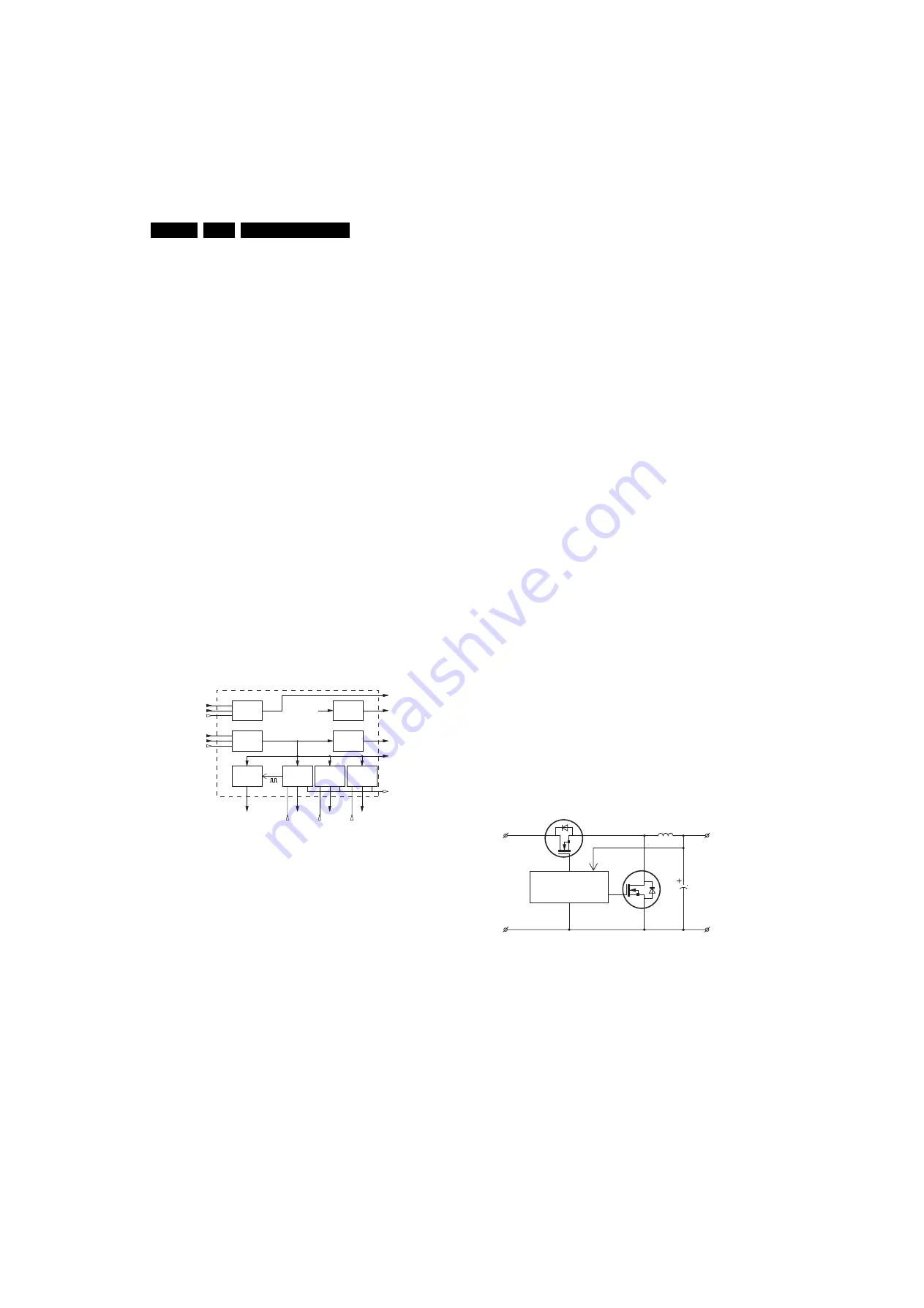
1.2V and 3.3V DC/DC Converters
Introduction
The circuit used is a so-called "synchronous buck converter".
Some characteristics:
•
Switching frequency: approx. 250 kHz.
•
Efficiency: approx. 90%.
•
Built-in output over-voltage and over-current protections
•
Soft start.
•
Software controlled “on/off” (via ENABLE line).
Block Diagram
Figure 9-4 Block diagram synchronous buck converter.
The advantage of a "synchronous buck converter" over a
"classical buck converter" is its better efficiency (about 90%).
The difference between the two is that in a synchronous buck
converter the "low -side" diode is replaced by a MOSFET TS2
(item 7U03). This, because the voltage drop across a MOSFET
is smaller than the forward voltage drop of a diode.
This second MOSFET TS2 conducts current during the "off"
times of the first MOSFET TS1 (item 7U01 at the input side).
8V6
SWITCH
+5V
+8V6
+8V6-SW
+2V5D
+2V5
+12VSW
SUPPLY-FAULT
ON-MODE
+2V5D
LINEAR
STABILISER
+5V2_STBY
12V
SWITCH
+12VSW
+1V2
ENABLE-1V2
VSW
VTUN
GENERATOR
12V/1V2
DC/DC CONV.
12V/3V3
DC/DC CONV.
+12VS
+5V
POD-MODE
+2V5
LINEAR
STABILISER
+3V3
VTUN
ENABLE-3V3
F_15400_004.eps
280905
(Reserved)
(Reserved)
(Reserved)
12V/2V5
DC/DC CONV.
+2V5
ENABLE-2V5
F_15400_005.eps
090505
D
S
G
D
Vin
S
G
PWM GENERATOR
& MOSFET DRIVER
GND
Vout
GND
C1
TS2
FB
TS1
L1


