Circuit Descriptions, Abbreviation List, and IC Data Sheets
EN 162
BJ2.4U/BJ2.5U LA
9.
allow selection of the output out of five L+R inputs, two mono
signals (AM internal or AM external) and two externally
connected DSND streams.
SIF Switching
SIF (Sound Intermediate Frequency) switching allows
selecting between internal or external SIF signals.
AD Converters
The second part of the MPIF is responsible for conversion of
the chosen signals into digital signals and grouping them into
three data streams. Each data stream handles both video and
audio. These data streams are fed into three data links and
send via I2D to the outside.
The MPIF contains four video ADCs for analog and digital
video broadcast signals. The clock frequency for these ADCs
is either 27 MHz or 54 MHz. In some cases, two analog signals
are multiplexed at the input of one ADC. In these cases, the
clock frequency of the ADCs is 54 MHz, while the sample
frequency for each of the two signals is 27 MHz.
The sample frequency for standard 1fH video signals is 27
MHz. For the YUV channel the sample frequency of the U and
V components is half the sample frequency of the Y signal.
For 2fH YPbPr or RGB input signals (for instance 480p or 1080i
ATSC signals), the frequency that is used to sample the YUV
signals is twice as high as for 1fH signals. The sample
frequency is 54 MHz for Y and 27 MHz for U and V.
Due to the high sample frequency, two data links are needed
for transport of the video data to the digital video processor.
I
2
D Data Link
The digital interface between MPIF and AVIP is called Data
Link (or I
2
D Link). This is a serial interface that transfers the
data from MPIF to AVIP over three Data Link interfaces. Each
Data Link has a data signal and a strobe signal. The
synchronization information is distributed over the data and the
strobe signal. To minimize EMC, both signal outputs are low
voltage differential swing signals, with a swing of about 300
mV.
Each Data Link has four lines, one differential pair for the data,
and one differential pair for the strobe. The data rate is 594
Mbit/s. Each Data Link can carry two 27 MHz sampled video
streams (or one 54 MHz sampled 2fH video stream) and two
audio channels sampled at 6.75 MHz.
In the MPIF, the (video and audio) data to be transmitted is
multiplexed in an output register of 44 bits (including the 2 bit
sync information). The content of that 44 bits register is serial
transmitted on one of the three data links. In the AVIP, the
serial data is de-multiplexed into parallel streams. The data on
the data link is divided in several groups of signals (video, audio
and strobe signals). Obvious it is important that the transmitter
and receiver are in the same transmitting mode
Data links can operate in two different modes called:
1.
Normal mode.
2.
YUV2fH.
Normal Mode
In the normal mode the content of the data links is as follows:
Table 9-2 Normal mode
In the normal mode the data links can handle up to three video
signals: CVBS or YC signal from the primary video selector,
CVI 1fH source selected on the CVI switch, and CVBS signal
from the secondary video selector.
YUV 2fH Mode
In the YUV 2fH mode (higher bandwidth signal) the data links
content is as follows:
Table 9-3 YUV 2fH mode
The data link 1 can output only one of two input signals: the
output of the primary video selector or the Y output of the CVI
switch. Only one can be active at a moment, and that is
determined by the data link mode bit (DM). It means, that for
data links working in YUV 2fH mode, the data link 1 carries the
Y component of the YUV 2fH signal, the data link 2 carries the
UV component, and the data link 3 contains the signal that is
connected through the secondary video selector.
9.7
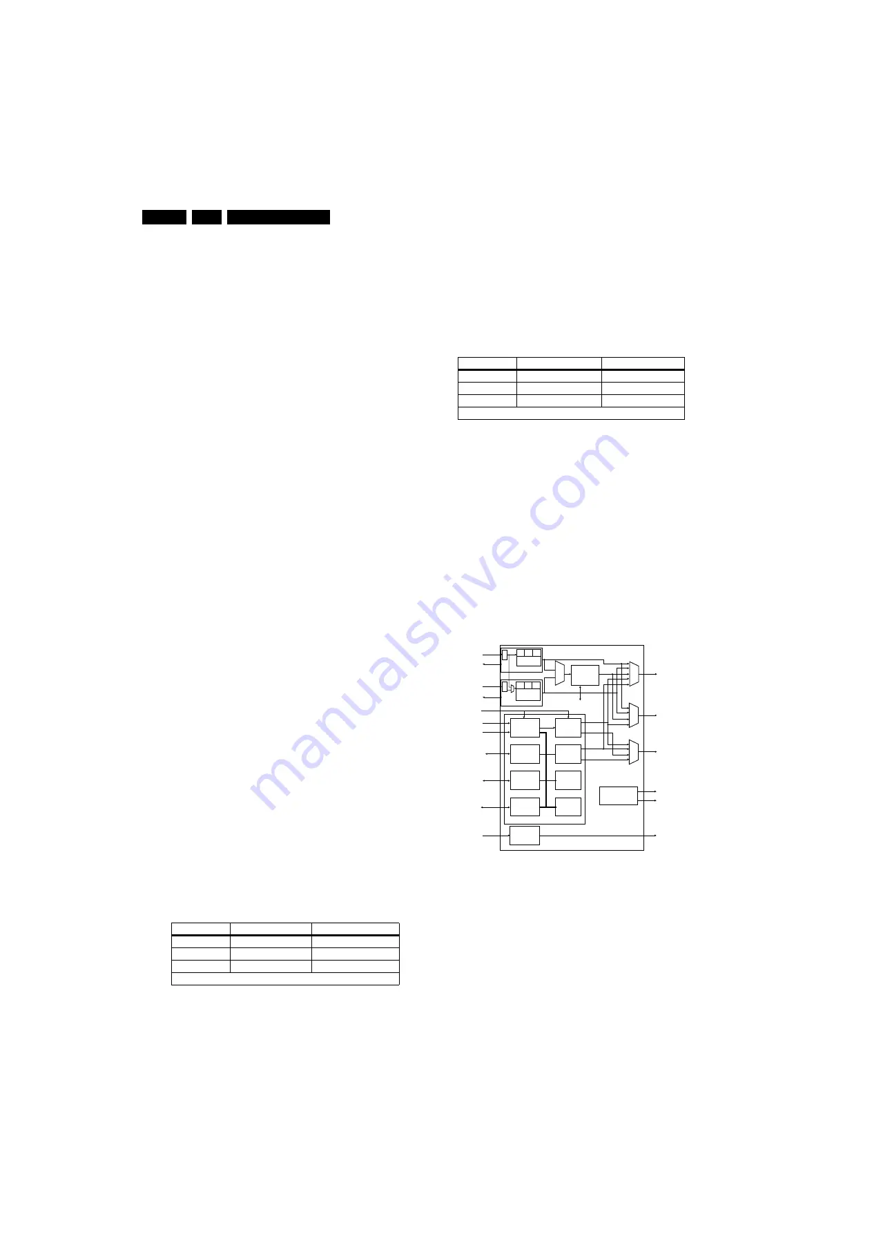
PNX2015
The functional blocks of the PNX2015 (item 7J00) are:
•
Audio Video Input Processor (AVIP).
•
3D Comb Filter (COLUMBUS).
•
High Definition MPEG Decoder (HD Subsystem).
•
LVDS transmitter.
•
Stand-by Processor for low-power control.
Figure 9-17 Block diagram PNX2015
These different blocks are described separately in the next
paragraphs.
Data Stream
Video
Audio
1
CVBS/YC primary
(L+R) primary
2
YUV 1fH
(L+R) secondary
3
CVBS secondary
SIF
Data link Mode bit: DM= 0
Data Stream
Video
Audio
1
Y 2fH
(L+R) primary
2
UV 2fH
(L+R) secondary
3
CVBS secondary
SIF
Data link Mode bit: DM= 1
AVIP-1
DLINK1
SYNC
COLUMBUS
0-9
10-19
VO-1
memory
controller
DV1
DV2
DV1MUX
DV3MUX
DV2MUX
PNX8550
direct
0-9
10-19
VO-2
HUB
PNX3000-1
AVIP-2
VIP
DLINK2
SYNC
PNX3000-2
DV4
DV5
video
SOUTH
TUNNEL
RX/TX
MBS
MEMORY
CONTROLLER
VMPG
LCD panel
PNX8550
DV3
PNX8550
NORTH
TUNNEL
RX/TX
LVDS_TX
TA, TB, TC, TD, TE, CLK
HD SUBSYSTEM
COLMUX
PNX2015
RGB,
HV
PNX8550
video
coprocessor
PNX8550
16-bit
200 MHz
DDR
D
L
I
N
K
D
L
I
N
K
VIDDEC
DCU
ITU
656
AUDIO
VIDDEC
DCU
ITU
656
AUDIO
TV
Microcontroller
PNX8550
Power Control
DSP/DEMDEC
DSP/DEMDEC
SYNC
F_15400_105.eps
180505
BLOCK DIAGRAM


