background image

Circuit Descriptions, Abbreviation List, and IC Data Sheets

EN 126

LC4.9E AA

9.

For the case of AP, the standard consists of BG/DK/I/M for 
a Multi-System set. The diversity here will then depend on 
the region. AP China can have a Multi-System and I/DK 
version. For India, it might only be BG standard.

9.8.2

Functionality

The features available in the Hercules are as follows:

Treble and Bass Control.

Surround Sound Effect that includes:

Incredible Stereo.

Incredible Mono.

3D Sound (not for AV Stereo).

TruSurround (not for AV Stereo).

Virtual Dolby Surround, VDS422 (not for AV Stereo).

Virtual Dolby Surround, VDS423 (not for AV Stereo).

Dolby Pro-Logic (not for AV Stereo).

Bass Feature that includes:

Dynamic Ultra-Bass.

Dynamic Bass Enhancement.

BBE (not for AV Stereo).

Auto-Volume Leveler.

5 Band Equalizer.

Loudness Control.

All the features stated are available for the Full Stereo versions 
and limited features for the AV Stereo 

9.8.3

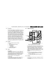
Audio Amplifier

The audio amplifier part is very straightforward. It uses two 
integrated TDA8931T power amplifiers for the L and R 
channels; each amplifier IC is able to deliver a maximum output 
of 20 W

RMS

 continuously in a 4-6 ohm speaker without needing 

a heatsink.
The operating supply for the amplifier may range from 12 V to 
32 V; in the LC04x TV set, depending on the model, supply 
voltages of 18 V (for the 5 W / 8 ohm version) or 24 V (for the 
15 W / 4 ohm version) are used. 
Muting is done via the SOUND_ENABLE line connected to pins 
7 of both amplifier-ICs, which comes from the Hercules.

9.8.4

Audio: Lip Sync

No Lip Sync adjustments are neccessary in this model.  

9.9

Control

9.9.1

Hercules

The System Board has two main micro-controllers on board. 
These are:

On-chip x86 micro-controller (OCM) from Genesis LCD or 
plasma TV/Monitor Controller.

On-chip 80C51 micro-controller from Philips 
Semiconductor UOCIII (Hercules) series.

Each micro-controller has it own I

2

C bus which hosts its own 

internal devices.
The Hercules is integrated with the Video and Audio Processor. 
For dynamic data storage, such as SMART PICTURE and 
SMART SOUND settings, an external NVM IC is being used.
Another feature includes an optional Teletext/Closed Caption 
decoder with the possibility of different page storage depending 
on the Hercules type number.

9.9.2

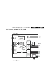
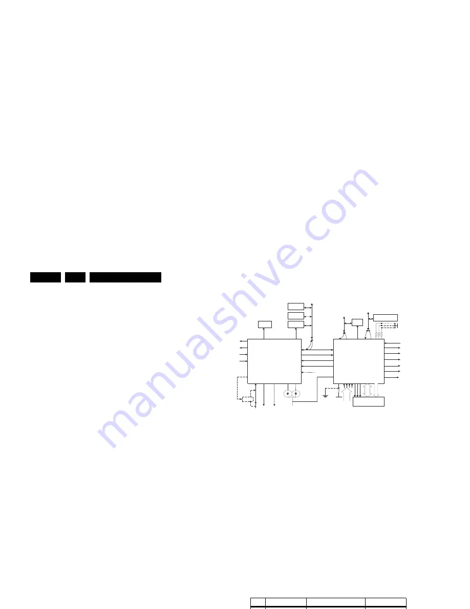
Block Diagram

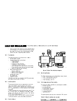
The block diagram of the Micro Controller application is shown 
below.

Figure 9-7 Micro Controller block diagram

9.9.3

Basic Specification

The Micro Controller operates at the following supply voltages:

+3.3 V

DC

 at pins 4, 88, 94, and 109. 

+1.8 V

DC

 at pins 93, 96, and 117.

I

2

C pull up supply: +3.3V

DC

.

9.9.4

Pin Configuration and Functionality

The ports of the Micro Controller can be configured as follows:

A normal input port.

An input ADC port.

An output Open Drain port.

An output Push-Pull port.

An output PWM port.

Input/Output Port

 
The following table shows the ports used for the LC04 control:

Table 9-2 Micro Controller ports overview

The description of each functional pin is explained below:

Pin

Name

Description

Configuration

97

INT0/ P0.5

IR

INT0

98

P1.0/ INT1

TV_IRQ

INT2

99

P1.1/ T0

TV_SC_COM

P1.1

102

P0.4/ I2SWS

EXT_MUTE

P0.4

103

P0.3/ I2SCLK

Lip Sync

I2SCLK

104

P0.2/ I2SDO2

NVM_WP

P0.2

105

P0.1/ I2SDO1

Lip Sync

I2SDO1

106

P0.0/ I2SDI/O Lip Sync

I2SDI/O

107

P1.3/ T1

PC-TV_LED

P1.3

108

P1.6/ SCL

SCL

SCL

109

P1.7/ SDA

SDA

SDA

111

P2.0/ TPWM

SOUND_ENABLE

P2.0

112

P2.1/ PWM0

(for future use)

-

113

P2.2/ PWM1

(for future use)

-

114

P2.3/ PWM2

SEL_IF

P2.3

115

P3.0/ ADC0

Light Sensor - SDM

ADC0

116

P3.1/ ADC1

STATUS_1

ADC1

119

P3.2/ ADC2

STATUS_2

ADC2

120

P3.3/ ADC3

KEYBOARD

ADC3

122

P2.4/ PWM3

STANDBY

P2.4

123

P2.5/ PWM4

(for future use)

-

126

P1.2/ INT2

(for future use)

-

127

P1.4/ RX

HERC_RESET

-

128

P1.5/ TX

POWER_DOWN

P1.5

HERCULES

SCALER

T

u

ner

ComPair

N

V

M

So

u

nd

Amp

MUX

N

V

M

GPROBE for De

bu

g

or ComPair(Scaler)

SDA

SCL

T

V

_IRQ

T

V

_SC_COM

+3

V

3STBY

1407

1406

1405

PC_DET

SD_PCHD_SEL

PC_HD_SEL

POWER_DOWN

LAMP_ON_OFF

PANEL_PWR_CTL

HD_FILTER

BACK_LIGHT_ADJ1

Flash ROM

83
GPIO2

N

V

M_WP

IIC BUS 2

                  93
               N

V

RAM

                _SDA

92
N

V

RAM

_SCL

72

71

187

193

194

85

(GPIO4)

88

(GPIO5)

89

(GPIO6)

68

(PBIAS)

67

(PPWR)

99

(PWM1)

98

(GPIO11/

PWM0)

78 DDC_SDA_

V

GA

77 DDC_SCL_

V

GA

82 GPIO1

81 GPIO0

+3

V

3STBY

111

GPIO23

90 GPIO7

ROM_ADD0-17

ROM_DATA0-7

 5   6   7

103 106 107 108

HIGH or
LOW
level inp

u

t

IIC BUS1

N

V

M_WP

So

u

nd_Ena

b

le

HREC

RST

Sel IF/
SDM

Stat

u

s1

Light
Sense

T

V

_IR

RC

P50_LINE_IT

V

_IR_SW

EXT_MUTE

Stand

b

y

POWER
DOWN

127
P1.4

114
P2.3

116
ADC1

115
ADC0

123
P2.5

97
INT0

102
P0.4

122
P2.4

126
INT2

128
P1.5

SDA 109

SCL 108

INT1 98

P1.1 99

Key

b

oard

ADC3 120

111
P2.0

104
P0.2

E_14490_062.eps

160904

Summary of Contents for 42PF5320/10

Page 1: ...tpoint Overviews and Waveforms Wiring Diagram 25 Block Diagram Video 26 Block Diagram Audio 27 Testpoint Overview Small Signal Board 6093 1 28 Testpoint Overview Small Signal Board 6141 1 29 I2C IC Overview 30 Supply Voltage Overview 31 SSB MUX Sync Interface B13 56 66 75 SSB Digital I O B14 57 66 75 SSB Analog I O B15 58 66 75 SSB Top Connectors B16 59 66 75 SSB Side Connectors B17 60 66 75 SSB A...

Page 2: ...Colour systems PAL B G D K I SECAM B G D K L L Video playback PAL B G SECAM L L NTSC M N 3 58 4 43 Supported computer formats VGA 640x480 VGA 720x400 VGA 720x480 MAC 640x480 MAC 832x624 SVGA 800x600 XVGA 1024x768 WXGA 1280x768 WXGA 1280x960 WXGA 1280x1024 Power consumption Normal operation W 450 Stand by W 2 Dimensions WxHxD cm 42 inch 124x68x10 4 50 in 141 5x78x10 4 Weight kg 42 inch 42 50 inch 5...

Page 3: ...ue 0 7 VPP 75 ohm j 15 Video Red 0 7 VPP 75 ohm j 16 Status FBL 0 0 4 V INT 1 3 V EXT 75 ohm j 17 Ground Video Gnd H 18 Ground FBL Gnd H 19 Video Terr CVBS 1 VPP 75 ohm k 20 Video CVBS Y 1 VPP 75 ohm j 21 Shield Gnd H EXT2 Video Y C in CVBS In Out Audio In Out Figure 1 5 SCART connector 1 Audio R 0 5 VRMS 1 kohm k 2 Audio R 0 5 VRMS 10 kohm j 3 Audio L 0 5 VRMS 1 kohm k 4 Ground Audio Gnd H 5 Grou...

Page 4: ... AA 1 1 3 Chassis Overview Figure 1 6 PWB locations PDP AUDIO AMPLIFIER PANEL C F_15430_044 eps 140605 A E SMALL SIGNAL BOARD B PLASMA DISPLAY PANEL POWER SUPPLY PANEL LOUDSPEAKER COMPARTMENT LOUDSPEAKER COMPARTMENT KEYBOARD CONTROL PANEL IR LED PANEL J SIDE I O PANEL D ...

Page 5: ...Power plug Check the cabinet for defects to prevent touching of any inner parts by the customer Service Default Mode see chapter 5 with a colour bar signal and stereo sound L 3 kHz R 1 kHz unless stated otherwise and picture carrier at 475 25 MHz for PAL or 61 25 MHz for NTSC channel 3 Where necessary measure the waveforms and voltages with D and without E aerial signal Measure the voltages in the...

Page 6: ... gets wet inside and during the heating time the structure of the IC will be destroyed due to high steam pressure inside the body If the packaging was opened before usage the IC has to be heated up for some hours around 90 C for drying think of ESD protection Do not re use BGAs at all For sets produced before 1 1 2005 containing leaded soldering tin and components all needed spare parts will be av...

Page 7: ...Directions for Use EN 7 LC4 9E AA 3 3 Directions for Use You can download this information from the following websites http www philips com support http www p4c philips com ...

Page 8: ...Dressing 4 2 Service Positions 4 3 Assy Panel Removal 4 4 Set Re assembly Notes Figures below can deviate slightly from the actual situation due to the different set executions Follow the disassembling instructions in described order 4 1 Cable Dressing Figure 4 1 Cable dressing F_15430_043 eps 080605 ...

Page 9: ...round the outer rim tapping screws around the connector plate 3 Remove the four mushrooms from the rear cover 4 Lift the metal rear cover from the set Make sure that wires and flat foils are not damaged 4 3 2 Speaker Compartment Cover After removing the metal rear cover you gain access to the Speaker Compartment covers 1 Remove all T10 screws 1 around the outer rim of the cover see Figure Speaker ...

Page 10: ...e assy 3 Remove the panel from its bracket 3 by pushing against the front side of the side I O cinch connectors Figure 4 7 Side I O panel removal When it is defective replace the whole unit 4 3 4 LED Panel Figure 4 8 LED panel 1 Remove the fixation screws 1 and take the panel out of its brackets 2 Disconnect the cable 2 from the panel 4 3 5 Keyboard Control Panel F_15430_048 eps 100605 2 1 3 F_154...

Page 11: ... the grounding cable 3 Remove the fixation screws 3 see Figure SSB board cover shield and remove the SSB shield with the SSB board inside and the rear I O panel still attached to it 1 Remove the two fixation screws 1 that secure the SSB board on the lower part of the SSB shielding see Figure SSB board 2 Remove the SSB panel 4 3 8 Power Supply Panel Figure 4 13 Power supply panel 1 Disconnect all c...

Page 12: ...o Amplifier Panel Figure 4 14 Class D audio amplifier panel 1 Disconnect all cables 1 from the panel 2 Pinch the plastic fixation clamps 2 firmly between your fingers and pull the panel upwards 3 Take the panel out of its brackets 3 F_15430_051 eps 100605 3 2 1 ...

Page 13: ...e Main Supply board Mains cable at the Main Supply board Side I O cable at SSB side fragile connector Cable at LED panel Keyboard cable at SSB side Audio Amplifier supply cable at the Main Supply board Loudspeaker cables incl ferrites at the Audio panel 4 Lift the metal frame together with all PWBs from the display panel see figure Frame lift 5 After removal of the frame lift the PDP from the set ...

Page 14: ...plate 1 Remove the PDP as described earlier 2 Remove the T10 screws 1 from the mounting frame 3 After removal of the frame you can lift the glass plate from the set Figure 4 17 Glass plate removal 4 4 Set Re assembly To re assemble the whole set execute all processes in reverse order F_15400_119 eps 200505 1 ...

Page 15: ...hassis It offers the possibilities of structured troubleshooting error code reading and software version readout for all chassis Minimum requirements for ComPair a Pentium processor a Windows OS and a CD ROM drive see also paragraph ComPair 5 2 1 Service Default Mode SDM Purpose To create a predefined setting for measurements to be How to Enter To enter SDM use one of the following methods Press t...

Page 16: ...imer The run timer counts normal operation hours but does not count standby hours 2 AAABCD X Y This is the software identification of the main microprocessor A the project name LC04 x B the region E Europe A Asia Pacific U NAFTA L LATAM C the software diversity Europe T 1 page TXT F Full TXT V Voice control LATAM and NAFTA N Stereo non dBx S Stereo dBx Asian Pacific T TXT N non TXT C NTSC ALL regi...

Page 17: ...rol transmitter Press the POWER button on the television set 5 3 Problems and Solving Tips Related to CSM 5 3 1 Picture Problems Note The problems described below are all related to the TV settings The procedures used to change the value or status of the different settings are described Picture too Dark or too Bright If The picture improves when you press the AUTO PICTURE button on the remote cont...

Page 18: ... PWBs are only a mouse click away Specifications ComPair consists of a Windows based fault finding program and an interface box between PC and the defective product The ComPair interface box is connected to the PC via a serial or RS 232 cable For this chassis the ComPair interface box and the TV communicate via a bi directional service cable via the service connector s The ComPair faultfinding pro...

Page 19: ... not possible to increase the size when processing high resolution LVDS signals 1280x768 Generally this tool is intended to determine if the SSB is working or not Thus to determine if LVDS RGB and sync signals are okay How to Connect Connections are explained in the user manual which is delivered with the tool Note To use the LVDS tool you must have ComPair release ERROR 0 0 0 0 0 No errors detect...

Page 20: ...s followed by a pause of 1 5 seconds 1 long blink of 1 5 seconds to finish the sequence The sequence starts again with 12 short blinks 5 7 Fault Finding and Repair Tips Notes It is assumed that the components are mounted correctly with correct values and no bad solder joints Before any fault finding actions check if the correct options are set 5 7 1 NVM Editor In some cases it can be handy if one ...

Page 21: ...r Future Usage as defined by software 0 0 0 Total Dec Values 59 59 59 Total Hex Values 3B 3B 3B Byte 1 175 dec 0 PSE PSE 0 0 0 1 OPC OPC 0 0 0 2 PRIS PRIS 0 0 0 3 CONTINUOUS FACTORY Continuous factory mode 0 0 0 4 WHITE PATTERN ON Last color pattern status in factory mode 0 0 0 5 SDM MODE Service default mode on off 0 0 0 6 SAM MODE Service Align mode on off 0 0 0 7 SVMA Scavm On Off 0 0 0 Total D...

Page 22: ...st status 1 1 1 1 Inc_Life_Time Inc_Life_Time 0 0 0 2 PC_Mode PC_Mode 0 0 0 3 HD_Mode HD_Mode 0 0 0 4 Tact_Switch Tact_Switch 0 0 0 5 Set_In_Special_Stby Set_In_Special_Stby 0 0 0 6 Hotel_OSDDisplay Hotel_OSDDisplay 0 0 0 7 Hotel_MonitorOut Hotel_MonitorOut 0 0 0 Total Dec Values 1 1 1 Total Hex Values 01 01 01 Byte 7 181 dec 0 Hotel_IconMode Hotel_IconMode 0 0 0 1 DBE DBE 1 1 1 2 SD SD 0 0 0 3 Se...

Page 23: ...lso check pin 12 LAMP_ON_OFF of 1J02 It should be HIGH during normal operation Note For faultfinding purposes it is important to know the following in Pixel Plus and Digital Crystal Clear models which have an ADC B18 and Columbus 3D combfilter B19 the digital input of the scaler is used for the digital video path Hercules output whereas the analogue RGB input analogue input of the scaler is only u...

Page 24: ...Service Modes Error Codes and Fault Finding EN 24 LC4 9E AA 5 Personal Notes ...

Page 25: ...FIER INVERTER INVERTER RIGHT SPEAKER LEFT SPEAKER PDP POWER SUPPLY E CONTROL BOARD 3P 1M01 3P 1K02 6P 1K00 11P 1M36 9P 1J04 10P 1J00 1M03 11P 1J01 1M46 31P 1J04 11P 1M46 10P 1M03 7P 1M02 7P 1M02 31P LVDS CONNECTOR 10P CN06 8P CN07 10P P5 4P P6 4P 1K00 8P P1 2P3 CN308 AC INLET F_15430_052 eps 281105 8735 8736 8102 8152 8120 8136 8146 8150 8103 8199 8900 8101 Tuner 1107 3P 1103 3P 1101 3P Compair UA...

Page 26: ...AF16 AF12 AE15 AF15 AE12 AF13 AE14 AF14 B10 A10 N4 N3 B9 A9 B8 A8 AL B6 AE10 D2 C2 B2 7217 TDA15021H RO GO BO Vsync_SDTV Hsync_SDTV INTF_Y_OUT INTF_U_OUT INTF_V_OUT SC1_B_CVI_Pb_IN SC1_FBL_IN_1 SC1_R_CVI_Pr_IN SC1_G_CVI_Y_IN 19 DVI D CONNECTOR 19 STATUS_2 8 STATUS_1 6 7 5SW_a VTUN 1 8 9 16 17 24 C5 C1 C2 C3 C4 28 8 27 26 25 7436 2 4 3 7436 1 2 1 N C EF 7L01 EF 7L03 EF 7L02 7L04 MST9883C A D CONV C...

Page 27: ... 6 6 LED2 LED1 RC 3061 5V2 STBY Red Green PC TV LED LED_SEL IR 5V2 STBY KEYBOARD 97 7217 TDA15021H 115 107 120 7430 3v3STBY 5VSW 3431 6F00 114 SEL_IF_SDM 4022 SERVICE SMD 116 STATUS_1 B3 119 STATUS_2 B3 MUTE OUT_MUTE 102 EXT_MUTE B5 POWER_DOWN SOUND_ENABLE 111 SOUND ENABLE B5 122 SC_STANDBY B15 B6 F_15430_053 eps 281105 B1 HERCULES 4110 6104 7101 3 SEL_IF_SDM B2 MUTE OUT_MUTE MUTE 4211 4212 1J04 3...

Page 28: ...201 A2 I202 A2 I203 B2 I204 B2 I205 B2 I206 B2 I207 B2 I208 B2 I209 B2 I210 A3 I211 A3 I212 A3 I213 A2 I214 B2 I215 A2 I216 B2 I217 B3 I218 A3 I219 B3 I220 B3 I221 A2 I222 A2 I223 A2 I224 A3 I225 A2 I226 B2 I227 B2 I228 B3 I229 B2 I230 A3 I231 B2 I232 A2 I233 B2 I234 B2 I235 B2 I236 B2 I237 B2 I238 A2 I239 A3 I240 A3 I241 A2 I242 A2 I243 A3 I244 B3 I246 A3 I247 A3 I248 A3 I254 C3 I255 B3 I256 B3 I...

Page 29: ...I213 B3 I214 C3 I215 B3 I216 C2 I217 C4 I218 B4 I219 B4 I220 C4 I221 B2 I222 B3 I223 B2 I224 B4 I225 B3 I226 C3 I227 C3 I228 B4 I229 C3 I230 B4 I231 C3 I232 B2 I233 C3 I234 C2 I235 B2 I236 B2 I237 B2 I238 B2 I239 B4 I240 B4 I241 A3 I242 A3 I243 B4 I244 C4 I246 B4 I247 B4 I248 B4 I254 E3 I255 B4 I256 C4 I257 B4 I258 C3 I259 C4 I262 B2 I264 B2 I265 C4 I266 C4 I267 C4 I268 B4 I269 B2 I270 C4 I271 B4 ...

Page 30: ... DVI D CONNECTOR 3102 5108 3101 5107 SDA_IO SCL_IO 5 6 7C01 M24C32 EEPROM P3 P4 3V3SW 3818 3817 ERR 8 NVM_WP_SCALER 7C00 MX29LV040 FLASH ROM 7B01 K4D263238F SDRAM ERR 14 ADDRESS DATA ADDRESS DATA AF5 N3 N4 SDA SCL 7 1107 1 2 3 SERVICE CONNECTOR UART UART_TX UART_RX 3122 3123 M1 M2 2 1802 1 JTAG_TDI_SDA JTAG_CLK_SCL AF7 AD6 3V3IO 3838 3837 JTAG I2C FSDATA FSADDR OCMDATA OCMADDR 7 SW_I2C_SDA SW_I2C_...

Page 31: ...SW 5VHDMI 5VHDMI 3V3SW 3V3SW 5VSWI 5VSWI 5VSWI 5VSWI DDC_5V 5F03 6F00 1 1F00 DVI_5V 3F20 6F01 5VSW 5VSW 3V3STBY 3V3STBY 5VSW 5VSW 5VSWIA 5VSWIA 3V3SWB 7K05 IN OUT COM 3V3SW 3V3SW 3V3SWA 5M03 5VSWI 5VSWI 5VSWIA 5M04 3V3SW 3V3SW 3V3 IO 3V3 IO 3V3SW 3V3SW 3V3 IO LVDS_VCC LVDS_VCC 1V5 7P01 IN OUT COM 5P01 5P02 5P03 1V5 PLL 1V5 INT 1K00 5 5K00 1K04 7 5K01 3V3STBY_1 5VSW_1 1 1J01 1M46 2 3 4 5 6 7 8 9 10...

Page 32: ...E7 I501 E3 I502 E4 I503 E5 I519 F9 I520 A6 6W7 680K 3507 I526 H11 I527 H10 RELAY CONTROL EMC HOLE 1405 1005 750mA F 0309 0 106451 1 9003 9004 3472 1K0 16V 100u 2541 I504 I513 9V_STBY_SW I509 I512 6460 BAS316 2001 470n 400V_HOT 500V B2P VA BF 0308 1 2 DSP 501N 1402 F503 3463 10K GROUND F508 I416 I406 1404 EMC HOLE I407 2003 470n 100 230VAC2 F500 I411 100u 2532 16V F501 2503 47u 400V 3400 2322595 I5...

Page 33: ...D8 I347 D8 I348 D8 I349 C9 I350 D9 I351 D9 I352 D10 I382 F1 15K 3074 I307 I344 16V 10u 2398 2387 100u 16V 47K 3398 3397 47K 47K 3394 47K 47K 3392 3393 1K0 3390 100R 3386 3399 3396 5K6 3320 10K 47K 3381 BAS316 6367 7004 P0102BL 560R 3356 10K 3353 7366 4 12 13 14 4 11 I381 LM324 5V_STBY_SW I380 100K 3395 I305 LM339P 5 4 2 3 12 7348 BC847BW 7330 3 BC857BW 7391 10K 3341 3342 10K BC847BW 7352 6335 F368...

Page 34: ...I613 E7 I614 B8 I662 H12 I663 G1 I664 I6 I665 I7 I666 I6 I667 I7 I668 I7 I616 G5 I617 G2 I618 H4 I619 H4 I620 H5 I621 G4 I633 H1 I634 B6 I641 E8 I642 E10 I643 G7 I644 G8 I645 G8 I646 G8 NFR25 NFR25 I660 330K 3684 I659 6640 SS14 I657 I645 I656 I653 I654 I602 I651 I650 3677 47K 3673 1K0 F601 I632 3671 10K 10n 2675 500V F605 50V 2613 1n0 BZG03 C18 6609 I642 I649 3621 2603 I615 I667 I668 BC369 7608 25...

Page 35: ...4 86V 6V 19382 19382 HOT U14 E6 0204 H9 1000 G6 F G 2008 F3 2009 E5 1008 G9 1 4 3 2070 1n0 TCET1102 G 7002 BAS316 6005 I020 I018 4K7 3012 6R8 3021 F293 I059 50V 2024 3n3 3043 4K7 6034 BAS316 3005 27K I074 F004 I079 2016 50V 2u2 100n 2047 6044 STTH2003C 1 3 2 200V 2028 220p 47p 2037 F295 GND4 F292 F007 F290 I039 3059 56K 3070 10K 6010 BAS316 50V 2010 10n 10K 3013 9007 BCP56 7013 6003 BZX384 C33 50V...

Page 36: ...69 H8 I245 I8 I246 B6 H I I134 B10 I135 C6 I136 B10 1M10 I235 G11 I236 G9 19382 39812 VA 6 1 I138 A9 I139 A7 I140 B8 I141 A8 F 6216 H8 I142 A6 0V5 1J01 G H I114 E2 I115 D2 I116 D2 I117 D3 7060 2 B11 0V5 DISPLAY RES I118 D4 I120 D8 I121 D7 I122 D10 I123 D9 I221 19382 NFR25 I243 I11 I244 I3 0R51 3145 BZX384 C18 6061 BYW29EX 200 6120 3062 1K0 12V 10K 3147 12V 1K0 3142 50V 2227 100p 3220 33R I114 470p...

Page 37: ...0 F5 3202 F6 3203 G6 3204 F5 3205 F5 3206 F5 3207 F5 3208 F5 3209 F5 3210 E8 3212 F6 3213 F6 3214 F6 3215 F6 3216 F6 3217 F6 3218 F6 3219 F5 3220 G6 3224 E8 3225 E8 3226 E8 3228 E8 3229 E8 3260 F8 3261 F8 3262 G8 3263 G8 3264 G8 3265 G8 3268 G8 3269 G7 3292 B8 3300 E6 3301 E6 3304 G7 3306 G7 3307 G7 3308 G6 3311 F8 3312 G7 3313 G7 3317 G7 3320 G7 3321 G7 3322 G7 3323 G7 3324 G7 3325 F7 3326 G7 332...

Page 38: ...38 LC4 9E AA 7 Circuit Diagrams and PWB Layouts Layout PDP FHP Supply Part 1 Top Side E_16040_036a eps 161205 Part 1 ...

Page 39: ...Circuit Diagrams and PWB Layouts 39 LC4 9E AA 7 Layout PDP FHP Supply Part 3 Top Side E_16040_036c eps 161205 Part 3 ...

Page 40: ...40 LC4 9E AA 7 Circuit Diagrams and PWB Layouts Layout PDP FHP Supply Part 3 Top Side E_16040_036c eps 161205 Part 3 ...

Page 41: ...Circuit Diagrams and PWB Layouts 41 LC4 9E AA 7 Layout PDP FHP Supply Part 4 Top Side E_16040_036d eps 161205 Part 4 ...

Page 42: ...42 LC4 9E AA 7 Circuit Diagrams and PWB Layouts Layout PDP FHP Supply Bottom View 3104 303 5016 1 E_16040_037 eps 271005 ...

Page 43: ...3124 I111 5VSW_a 5VSW_b 5VSW_b 5VSW_a VTUN 5VSW_a 2102 10n 16V 100u 2101 3106 16 17 7 8 6 9 10 13 14 15 2 3 11 12 1106 OFWK9656L 40M4 1 18 4 5 3V3STBY 5 6 1 2 3 4 F113 1103 F112 F116 F115 F117 3123 100R 100R 3122 6106 BZX384 C6V8 BZX384 C6V8 6107 6101 6102 BZX384 C6V8 BZX384 C6V8 F111 F110 F109 F114 3V3STBY 3120 10K 3 4 5 10K 3121 1107 1 2 1 2 3 4 5 1101 6 NC1 NC2 10 SCL 4 SDA 5 TU 2 11 12 13 14 1...

Page 44: ... F10 I266 F10 I267 F11 I268 G11 I269 C11 I270 B11 I271 B10 I272 B10 I273 C9 I274 A9 I275 A9 I277 C8 I278 C8 I283 B6 I284 B6 I285 B6 I288 B6 I289 A3 I290 A3 I291 A4 I292 B3 I293 B3 I294 B3 I297 B8 I298 C7 B15 B23 B15 B15 B23 B15 B23 B15 B23 B15 B23 B15 B23 B15 B23 SFSKA 1201 2 1 3 4M5 4202 4203 4201 4215 4213 4214 2293 2292 100n 4211 4212 100n 2285 4206 2291 5218 5VSW 3294 3293 3292 3291 150R 3282 ...

Page 45: ... B3 I454 B2 0V 3V1 I440 I453 I454 3463 2449 100n 3V3SW 3V3SW 100R 3462 100R 4439 3461 4441 100R 3459 3V3SW 4438 3V3SW 100R 3458 4440 3456 100R 100R 3454 100R 3455 13 7 14 12 3453 100R 14 10 7436 6 74LVC14APW 74LVC14APW 11 7 9 7 14 8 7436 5 74LVC14APW 5 7 14 6 7436 4 74LVC14APW 7 14 4 7436 3 7436 2 74LVC14APW 3 7436 1 74LVC14APW 1 7 14 2 3V3SW 3V3SW 4437 4436 I451 I452 I450 I443 I449 6431 1N4148 10...

Page 46: ... B8 2505 B9 2506 C10 2507 D10 2508 F6 2509 F7 3501 F6 3502 F6 4501 E2 4502 F2 4503 F2 4504 F3 4505 F3 4506 F3 4507 C9 4508 C9 4509 C9 22 28 27 F502 1 2 3 4 5 6 7 8 9 10 1 2 3 4 5 6 7 I505 8 9 10 I503 I504 20 11 12 13 15 16 17 18 19 14 9 10 24 25 26 1 2 3 4 5 21 23 6 7 8 CY62256LL 70ZC 7502 32kx8 RAM 82p 2508 470p 2507 20 330p 2506 11 1 19 18 17 16 15 14 13 12 2 3 4 5 6 7 8 9 10 12 20 74HC573PW 750...

Page 47: ... C4 I607 C4 I608 A5 I610 B5 I611 C7 I612 C6 I613 E3 I614 E4 I615 E4 I616 E8 I617 F5 I618 A6 I619 D8 470p 2604 2619 47u 4606 4621 5V 4620 4619 3V3STBY 4618 4617 4616 4615 4614 4613 4612 4611 4610 4609 3633 39R 39R 3632 5V 3628 3629 3631 470R 3630 470R 5VSW 22K 3627 10K 3626 I619 6601 I618 BZX384 C3V3 I617 I616 I614 I615 I613 I612 I610 I611 I608 4603 3K3 3625 4601 5VSW 5VSW 2614 100n 7606 2 BC847BS ...

Page 48: ...2738 G2 2739 G3 2741 G3 2750 F9 2751 B9 3761 100R 25V 1u0 2761 3760 25V 100R 16V 2760 1u0 3736 2731 470u SUP_GND1 SUP_GND1 4K7 2734 22n I760 SUP_GND1 LVDS_VCC 5VSWI SUP_GND1 SUP_GND1 3V3STBY 7756 PDTC114ET 1K0 3759 3750 3V3SW I748 22K 1 2 3 2750 2u2 SI4433DY 7758 5 6 7 8 4 F700 100p 2701 2700 5700 5V I758 I749 5VSWI I750 F755 I755 F754 I754 I751 I753 I752 I747 I757 I756 6 7 I759 1 2 3 4 5 SUP_GND3...

Page 49: ... COL R 7210 V V V V V TRA SIG SM BC847BW COL R 7217 V V IC SM TDA15011H N1BD0 PHSE Y 7217 V V V V V IC SM TDA15021H N1B91 PHSE Y 7219 V V V IC SM 74HC4053D PHSE R Item 26 32PFxxxx AP NAFTA LT EU AP DVB sets LC4 3E LC4 9x LC4 8x LC4 3A China 26PF4310 10 Description 2449 V V V CER2 0402 Y5V 16V 100N COL 3432 V RST SM 0402 2K7 PM5 COL 3458 V V V RST SM 0402 100R PM5 COL 3459 V V V RST SM 0402 100R PM...

Page 50: ...GRN1 AE5 GPIO_G09_B4 DEBLU0 AF5 GPIO_G09_B5 DEBLU1 AE9 GPIO_G07_B4 DERED6 AF9 GPIO_G07_B5 DERED7 AD10 GPIO_G07_B6 DERED8 AE10 GPIO_G07_B7 DERED9 AD6 GPIO_G08_B0 JTAG_CLK DORED0 AE6 GPIO_G08_B1 JTAG_MODE DORED1 AF6 GPIO_G08_B2 JTAG_TDI DOGRN0 AE7 GPIO_G08_B3 DVS DOGRN1 AC18 GPIO_G06_B0 DORED2 AD18 GPIO_G06_B1 DORED3 AE18 GPIO_G06_B2 DORED4 AF18 GPIO_G06_B3 DORED5 GPIO_G07_B0 DERED2 AE8 AF8 GPIO_G07...

Page 51: ...RX0p B9 RX1n C6 C8 C9 C10 C11 A7 A11 B5 B7 C7 7801 2 GM1501 LF BD DVI D6 D8 D9 D10 4900 2942 100n B12 LBADC_IN2 A12 LBADC_IN3 D12 LBADC_RETURN 3V3_LBADC ADC GM1501 LF BD C13 D13 C12 LBADC_IN1 A1 C5 D5 AC17 K3 F1 7801 3 7801 14 GM1501 LF BD NC LVDSB_3 3_1 AD12 LVDSB_3 3_2 AD13 LVDSB_3 3_3 AC12 LVDSB_GND_1 AC13 LVDSB_GND_2 AC14 LVDSB_GND_3 AC15 VDDD33_LVDS AE17 VSSD33_LVDS AD17 LVDSA_3 3_1 AD20 LVDS...

Page 52: ...F13 BCp DEGRN8 AE12 SHIELD0 DEGRN2 AF10 SHIELD1 DEGRN3 AC11 SHIELD2 DEGRN4 AD11 AE19 ACn GPIO_G06_B7 DORED9 AF20 ACp GPIO_G06_B6 DORED8 AE20 B0n DEBLU9 AE16 B0p DEBLU8 AF16 B1n DEBLU7 AE15 B1p DEBLU6 AF15 B2n DEBLU4 AE14 A0n GPIO_G05_B7 DOGRN9 AF23 A0p GPIO_G05_B6 DOGRN8 AE23 A1n GPIO_G05_B5 DOGRN7 AF22 A1p GPIO_G05_B4 DOGRN6 AE22 A2n GPIO_G05_B2 DOGRN4 AF21 A2p GPIO_G05_B1 DOGRN3 AE21 A3n GPIO_G0...

Page 53: ...91 39 40 41 42 43 44 1 83 84 3 4 6 7 60 61 94 17 18 20 21 74 75 77 78 80 81 63 64 68 69 71 72 9 10 12 13 100 55 53 54 28 23 56 24 57 97 98 34 47 48 49 50 51 45 29 30 26 7B01 K4D263238F UC50 1M X 32 X 4 SDRAM Φ 31 32 36 37 33 2V5_DDR 2B16 100n 2B15 100n 100n 2B14 2B13 100n 2B11 100n 100n 2B12 100n 2B10 2B09 100n 100n 2B08 2B07 100n 100n 2B06 2B05 100n 100n 2B04 2B03 100n 2B02 47u 6 3V 16V 47u 2B01 ...

Page 54: ...C14 3C15 10K 3C04 4 4 5 3C04 3 10K 3 6 10K 3C04 2 2 7 1 8 3C04 1 10K FC10 FC07 FC06 FC09 FC08 FC05 FC04 FC02 FC03 FC01 3V3SW FC00 3C06 4 10K 4 5 10K 3 6 2 7 3C06 3 1 8 3C06 2 10K 4 5 3C06 1 10K 3 6 10K 3C07 4 10K 3C07 3 10K 3C07 2 2 7 10K 3C07 1 1 8 4 5 3 6 3C08 4 10K 2 7 3C08 3 10K 1 8 3C08 2 10K 3C08 1 10K 100n 2C00 3C18 10K 3C21 3C20 3C16 4 4 5 3V3_IO 3C16 3 3 6 2 7 10K 1 8 3C16 2 3C16 1 3C19 4...

Page 55: ...T APPLICABLE IN EUROPE SET 100K 3D34 100K 3D35 ID20 ID21 3V3SW 5 14 15 4 9 16 7 8 13 1 3 12 2 7D05 HEF4053B 6 11 10 2D45 1u0 MDX 2D44 1u0 ID18 ID19 FD16 4D01 ID16 4D00 ID17 3D30 3D31 3D32 3D33 3V3SW ID14 ID07 ID13 ID06 ID02 ID05 FD04 FD03 FD12 FD02 FD01 FD14 FD13 FD17 FD15 FD06 FD11 FD05 FD10 FD08 FD09 FD07 ID22 FD00 ID03 ID04 ID01 ID00 ID09 ID08 ID12 ID10 ID11 ID15 5VHDMI 2D01 10n 390R 3D10 3D11 ...

Page 56: ... IE04 3 4 5 6 2E39 15p 15p 2E38 2E37 15p 4E13 4E14 4E12 3E53 47K 47K 3E54 3E55 47K 47K 3E50 3E51 47K 47K 3E52 3E49 22R IE34 IE32 IE33 IE31 IE29 IE30 IE28 IE37 IE35 IE36 IE26 IE27 IE25 IE23 IE24 IE22 IE20 IE21 IE19 IE17 IE18 IE16 IE14 IE15 IE13 IE11 IE12 IE10 IE09 4E10 4E11 330R 3E18 3E17 330R 330R 3E16 56R 3E00 56R 3E01 56R 3E02 2E35 4u7 4u7 2E33 2E34 4u7 IE07 IE08 IE06 IE05 FE08 5E02 100n 2E15 2E...

Page 57: ...C2 2F07 C3 2F08 E2 2F09 E2 2F10 E3 2F11 F2 RX2 IN 1 2 3 4 5 6 7 8 9 10 1 2 3 4 5 6 7 17 18 19 20 21 22 23 24 16 1F00 3 ROW_C YKF45 7005 9 10 11 12 13 14 15 31 32 29 30 1F00 2 ROW_B YKF45 7005 1F00 4 YKF45 7005 C1 25 C2 26 C3 27 C4 28 4 5 6 7 8 YKF45 7005 ROW_A 1F00 1 1 2 3 7 8 YKB21 5101A 1F01 1 2 3 4 5 3F29 100R 3F28 100R IF23 IF20 IF22 IF15 IF17 IF14 IF12 IF13 IF11 FF13 IF21 FF12 FF10 FF11 FF09 ...

Page 58: ...12 13 14 15 1 2 3 4 5 6 7 8 9 10 11 12 13 14 15 A B C D E F G H I J K A B C D E F G H 6G10 BZX384 C3V9 6G09 BZX384 C3V9 6G08 6G07 BZX384 C3V9 BZX384 C3V9 BZX384 C3V9 6G04 6G03 BZX384 C3V9 BZX384 C3V9 6G06 BZX384 C3V9 6G05 3G09 4G22 4G21 IG80 4G20 5VSW 47K 3G95 47K 3G94 2G66 4u7 4G19 5VSW IG79 3G93 47K 3G92 47K 4u7 2G65 1G02 2 MT HR AR0761S 2 22 23 1G01 2 MT HR AR0761S 2 22 23 150R 3S01 9 33 34 4G1...

Page 59: ... 2J29 C7 2J30 F2 2J31 D2 2J33 C2 2J34 C3 B C D E F A B C D E F 1J00 B1 1J01 C1 1J02 D1 1J03 F1 1J04 B8 1J05 C8 1J06 E8 1 2 3 4 5 6 7 8 1 5V 12VUNREG 2 3 4 5 6 7 8 A 1n0 4J02 2J36 1J08 T 3A 1J07 1n0 2J35 IJ12 IJ13 4J01 2J33 2J34 5J05 1n0 2J31 5J04 2J30 1n0 5J03 5J02 100p 2J27 2J28 100p 100p 5J01 2J26 100p 2J29 2J02 1n0 2J23 100p 2J21 100p 2J22 100p 2J20 68R 3J05 3J06 100p 2J19 100p 2J17 68R 3J04 2J...

Page 60: ...1 12 13 14 15 16 17 18 1K03 4K06 4K07 3V3STBY_1 4K05 4K04 4K03 4K01 100p 2K28 2K27 100p 2K26 2K25 100p 100p 2K24 100p 2K22 100p 100p 2K23 100p 2K21 5K02 1u0 68R 3K13 3K12 68R 68R 3K11 2K19 1n0 2K20 1n0 1u0 5K01 2K18 100p IK18 IK17 11 2 3 4 5 6 7 8 9 FK11 1 10 B6B PH K 1K00 1 2 3 4 5 6 1K04 3V3STBY_1 5VSW 4K02 3V3STBY 2K01 2K00 1n0 1n0 5K00 1u0 B3B PH K S LF 1 2 3 1K02 FK08 FK09 IK16 IK03 IK01 IK02...

Page 61: ... 4L05 5VSWIA 3L39 3L38 7L08 3L08 3L11 150R 7L02 BC847BW 5VSWIA IL19 IL17 IL18 IL16 2L38 4L04 5L03 10u 82p 2L39 68p 2L37 3V3SWB 3V3SWB 3L37 3K3 3V3SWB 3K3 3L36 BSN20 7L07 3 1 2 3 1 2 7L06 BSN20 2L36 2L35 100n 2L33 2L34 100n IL14 IL15 IL13 IL12 IL10 IL11 IL08 IL09 IL07 2L31 100u 16V 16V 100u 2L32 3V3SWB 5VSWIA 16V 10u 2L30 7L05 LD1117DT33 1 3 2 4L03 3L35 220R 3L34 3L33 220R IL06 IL04 IL05 IL02 IL03 ...

Page 62: ... 2K7 3M71 5VSWIA 1 2 14 15 8 13 4 3 16 5VSWIA 7M15 1 74HCT221D 1n0 2M61 2M60 1n0 10K 3M69 5VSWIA 15K 5VSWIA 3M68 5VSWIA 10 6 7 8 5 12 11 16 5VSWIA 16 7M14 2 74HCT221D 9 74HCT221D 1 2 14 15 8 13 4 3 7M14 1 3M28 3M29 3M27 3M26 IM00 3M00 5M01 5M00 4M09 4M08 3M78 1K0 2M19 100n 100n 2M18 2M17 100n 2M16 100n 100n 2M15 100n 2M14 2M13 100n 100n 2M12 2M11 100n 100n 2M09 2M10 100n 100n 2M08 100n 2M07 100n 2...

Page 63: ...R 3N43 3N42 100R 3N44 2N19 100p FN23 FN24 FN21 FN22 3N29 FN20 100R 3N28 180R 3N27 47R TLMG3100 3V3 IO T15 IO_88 R15 6N01 M11 IO_80 M12 P12 IO_81 IO_82 R12 IO_83 T13 IO_84 R13 IO_85 R14 IO_86 P13 IO_87 T11 IO_72 N10 IO_73 P10 IO_74 R11 IO_75 P11 IO_76 N11 IO_77 N12 IO_78 M9 IO_79 N8 IO_64 P8 IO_65 M10 IO_66 R9 IO_67 T9 IO_68 P9 IO_69 N9 IO_70 R10 IO_71 M7 IO_56 T6 IO_57 R7 IO_58 P7 IO_59 N7 IO_60 R...

Page 64: ...DM83R 7P02 IO_93 N15 IO_94 N16 IO_95 K12 IO_96 K14 IO_97 L12 IO_98 N14 IO_129 C15 IO_130 C14 IO_131 D13 IO_89 N13 IO_90 P14 IO_91 P15 IO_92 R16 D15 IO_122 E14 IO_123 F12 IO_124 E13 IO_125 D14 IO_126 H13 IO_127 G12 IO_128 B16 IO_114 F16 IO_115 F14 IO_116 F13 IO_117 F15 IO_118 E16 IO_119 E15 IO_120 D16 IO_121 L16 IO_107 K16 IO_108 K15 IO_109 J16 IO_110 H12 IO_111 G14 IO_112 G13 IO_113 G15 IO_100 M14...

Page 65: ... V V V FXDIND 0805 100MHZ 30R COL R 5P03 V V V FXDIND 0805 100MHZ 30R COL R 5P04 V V V FXDIND 0805 100MHZ 30R COL R 5P05 V V V FXDIND 0805 100MHZ 30R COL R 5P06 V V V FXDIND 0805 100MHZ 30R COL R 6N01 V V V LED VS SM TLMG3100 VISH R 7N01 V V V IC SM EPCS4SI8N ALT0 R 7N02 V V V IC SM EP1C12F256C8N ALT0 Y 7N03 V V V TRA SIG SM BC847BS PHSE R 7N04 V V V IC SM THC63LVDF84B THIN R 7P01 V V V IC SM LF15...

Page 66: ...A3 3736 A3 3740 B3 3741 B3 3742 B3 3743 B3 3750 A5 3755 A5 3758 A6 3759 A5 3760 A5 3761 A5 3800 B5 3817 B5 3818 B5 3820 C6 3822 C6 3823 C6 3824 C5 3825 B5 3826 B5 3827 B5 3828 B5 3829 B5 3830 B5 3831 B5 3832 B5 3833 B5 3834 B5 3835 B5 3836 B5 3837 B5 3838 B5 3839 C6 3840 C6 3841 B6 3900 B6 3901 B5 3902 B5 3903 B5 3904 B5 3A02 C6 3A03 C6 3A04 C6 3A05 C6 3A06 C6 3C00 B5 3C01 B5 3C02 C5 3C03 C5 3C04 ...

Page 67: ...Circuit Diagrams and PWB Layouts 67 LC4 9E AA 7 Layout Small Signal Board Top Side Part 1 Part 1 F_15430_025a eps 180405 ...

Page 68: ...68 LC4 9E AA 7 Circuit Diagrams and PWB Layouts Layout Small Signal Board Top Side Part 2 Part 2 F_15430_025b eps 180405 ...

Page 69: ...Circuit Diagrams and PWB Layouts 69 LC4 9E AA 7 Layout Small Signal Board Top Side Part 3 F_15430_025c eps 180405 Part 3 ...

Page 70: ...70 LC4 9E AA 7 Circuit Diagrams and PWB Layouts Layout Small Signal Board Top Side Part 4 F_15430_025d eps 180405 Part 4 ...

Page 71: ... A1 2P42 A1 2P43 A1 2P44 A1 2P45 A1 3126 B6 3127 B6 3207 B6 3214 B6 3215 B5 3216 B5 3217 B5 3222 A5 3223 A5 3224 A5 3225 A5 3226 A5 3227 A5 3230 A6 3231 A6 3234 A6 3235 A6 3236 A6 3242 B5 3244 B5 3245 B6 3262 B6 3263 B6 3264 B6 3265 B6 3266 B6 3267 B6 3268 B5 3270 A5 3271 B5 3272 B6 3273 B6 3274 B6 3277 B5 3278 B5 3279 B5 3280 B6 3281 B6 3282 C5 3285 B6 3286 B5 3291 B5 3292 C5 3293 B5 3294 C5 3295...

Page 72: ...72 LC4 9E AA 7 Circuit Diagrams and PWB Layouts Layout Small Signal Board Bottom Side Part 1 Part 1 F_15430_024a eps 180405 ...

Page 73: ...Circuit Diagrams and PWB Layouts 73 LC4 9E AA 7 Layout Small Signal Board Bottom Side Part 2 Part 2 F_15430_024b eps 180405 ...

Page 74: ...74 LC4 9E AA 7 Circuit Diagrams and PWB Layouts Layout Small Signal Board Bottom Side Part 3 Part 3 F_15430_024c eps 180405 ...

Page 75: ...Circuit Diagrams and PWB Layouts 75 LC4 9E AA 7 Layout Small Signal Board Bottom Side Part 4 Part 4 F_15430_024d eps 180405 ...

Page 76: ...2 6107 F2 7101 D5 7102 D7 7103 E6 F101 B1 F102 B1 F103 C2 F104 C1 F105 C3 F106 D1 F107 D2 F108 A4 F109 D4 F110 B9 F111 B9 F112 E9 F113 E9 F114 F7 F115 F3 F116 F3 F117 F3 I101 C2 I102 B6 I103 C5 I104 D5 I105 D5 I106 D6 I107 E5 I108 E6 I109 F6 I110 D7 I111 E5 I112 C1 I113 C1 RES RES NC1 10 NC2 SCL 4 SDA 5 2 TU 1 AGC 3 AS 11 IFOUT 12 13 14 15 16 17 6 UV1318ST AIH MK3 TUNER 9 33V 7 5V ADC 8 100R 3101 ...

Page 77: ...2258 G4 2259 G7 2260 G7 2262 G7 B C D E F G H 1201 B6 1202 G9 2201 A3 2202 B3 2203 D2 2205 G4 2206 G4 2207 G4 2208 H3 2209 H4 2210 C5 2211 C5 2214 C6 2216 C6 2218 A6 2219 B6 2220 C7 2221 B7 2223 B8 2224 C8 2225 B9 2226 C9 2227 B10 2228 D4 2229 D5 3 1 2 3 4 5 6 7 8 9 10 11 1 2 3 4 5 6 7 8 9 10 11 A B C D E F G H A 4M5 SFSKA 1201 2 1 4203 4202 4215 4201 4213 4214 2293 2292 100n 4212 4211 100n 2285 4...

Page 78: ... C6 9 I454 B2 2448 3463 I440 4K7 3451 5VSW 13 7 14 12 7436 6 74LVC14APW 3V3SW 100R 3455 5 7 14 6 7436 3 74LVC14APW 100R 3459 3431 1K0 BZX384 C2V7 6430 3432 7430 PDTC114ET I430 3V3SW 4438 BM05B SRSS TBT 1 2 3 4 5 6 7 1440 2 3456 100R 7436 1 74LVC14APW 1 7 14 I443 2449 100n 4441 3461 100R 3453 100R 4437 5V 3V3SW 7 14 4 10 7436 2 74LVC14APW 3 11 7 14 7436 5 74LVC14APW 2447 10p 5 I452 B3B PH SM4 TBT L...

Page 79: ...1 A1 2502 B2 2503 D1 2504 B7 2505 B9 2506 D10 2507 D10 2508 F6 2509 F7 3501 F6 3502 F6 4501 E2 4502 F2 4503 F2 4504 F2 4505 F3 4506 F3 4507 C9 4508 C9 4509 C9 1 2 3 4 5 6 7 8 9 10 1 2 3 4 5 6 7 8 9 10 I504 I505 I503 22 28 27 F502 20 11 12 13 15 16 17 18 19 14 9 10 24 25 26 1 2 3 4 5 21 23 6 7 8 CY62256LL 70ZC 7502 32kx8 RAM 82p 2508 470p 2507 20 330p 2506 11 1 19 18 17 16 15 14 13 12 2 3 4 5 6 7 8...

Page 80: ...2611 C6 2612 F9 2613 C8 2614 C8 2615 B9 2616 B4 2617 C4 2618 B8 2619 F5 1 2 3 4 5 6 7 8 9 1 2 3 4 5 6 47u 2619 5V 4606 4621 4619 4620 4618 4617 3V3STBY 4616 4614 4615 4613 4611 4612 4610 39R 3633 4609 3632 39R 3628 5V 470R 3629 3631 3630 470R 22K 5VSW 10K 3627 3626 I619 I618 I616 6601 BZX384 C3V3 I617 I614 I615 I612 I613 I611 I608 I610 4603 3625 3K3 4601 5VSW 100n 2614 5VSW BC847BS 7606 2 7606 1 B...

Page 81: ...8 G1 2739 G2 2741 G2 2762 22u16V 100n 2751 3761 100R 25V 1u0 2761 3760 25V 100R 16V 2760 1u0 3736 2731 470u SUP_GND1 SUP_GND1 4K7 2734 22n I760 SUP_GND1 LVDS_VCC 5VSWI SUP_GND1 SUP_GND1 3V3STBY 7756 PDTC114ET 1K0 3759 3750 3V3SW I748 22K 1 2 3 2750 2u2 SI4433DY 7758 5 6 7 8 4 F700 100p 2701 2700 5700 5V I758 I749 5VSWI I750 F755 I755 F754 I754 I751 I753 I752 I747 I757 I756 6 7 I759 1 2 3 4 5 SUP_G...

Page 82: ...GRN1 AE5 GPIO_G09_B4 DEBLU0 AF5 GPIO_G09_B5 DEBLU1 AE9 GPIO_G07_B4 DERED6 AF9 GPIO_G07_B5 DERED7 AD10 GPIO_G07_B6 DERED8 AE10 GPIO_G07_B7 DERED9 AD6 GPIO_G08_B0 JTAG_CLK DORED0 AE6 GPIO_G08_B1 JTAG_MODE DORED1 AF6 GPIO_G08_B2 JTAG_TDI DOGRN0 AE7 GPIO_G08_B3 DVS DOGRN1 AC18 GPIO_G06_B0 DORED2 AD18 GPIO_G06_B1 DORED3 AE18 GPIO_G06_B2 DORED4 AF18 GPIO_G06_B3 DORED5 GPIO_G07_B0 DERED2 AE8 AF8 GPIO_G07...

Page 83: ...VI_SDA GPI_08 N3 REXT B11 RX0n B8 RX0p A8 RX1n B9 RX1p A9 D10 C6 C8 C9 C10 C11 A7 A11 B5 B7 C7 DVI GM1501 LF BD 7801 2 D6 D8 D9 4900 100n 2942 B12 LBADC_IN3 A12 LBADC_RETURN D12 3V3_LBADC ADC 7801 3 C13 D13 LBADC_IN1 C12 LBADC_IN2 A1 C5 D5 AC17 K3 F1 GM1501 LF BD VSSD33_LVDS NC GM1501 LF BD 7801 14 LVDSA_GND_3 AD12 LVDSB_3 3_1 AD13 LVDSB_3 3_2 AC12 LVDSB_3 3_3 AC13 LVDSB_GND_1 AC14 LVDSB_GND_2 AC1...

Page 84: ...4A02 SHIELD2 DEGRN4 AE11 SHIELD3 DEGRN5 AE13 SHIELD4 DEBLU2 AD14 SHIELD5 DEBLU5 AF14 B2p DEBLU3 AF12 B3n DEGRN7 AF11 B3p DEGRN6 AF13 BCn DEGRN9 AE12 BCp DEGRN8 AF10 SHIELD0 DEGRN2 AC11 SHIELD1 DEGRN3 AD11 AE19 A3p GPIO_G06_B4 DORED6 AF20 ACn GPIO_G06_B7 DORED9 AE20 ACp GPIO_G06_B6 DORED8 AE16 B0n DEBLU9 AF16 B0p DEBLU8 AE15 B1n DEBLU7 AF15 B1p DEBLU6 AE14 B2n DEBLU4 AF23 A0n GPIO_G05_B7 DOGRN9 AE2...

Page 85: ...96 2 95 8 14 22 59 67 39 40 41 42 43 44 87 88 27 93 15 4 6 7 60 61 94 52 38 89 90 91 75 77 78 80 81 1 83 84 3 72 9 10 12 13 100 17 18 20 21 74 56 24 57 97 98 63 64 68 69 71 51 45 29 30 26 55 53 54 28 23 31 32 36 37 33 34 47 48 49 50 2V5_DDR Φ SDRAM 1M X 32 X 4 K4D263238F UC50 7B01 100n 2B16 100n 2B15 2B14 100n 2B13 2B12 100n 100n 100n 2B11 2B10 100n 100n 2B09 2B08 100n 100n 2B07 2B06 100n 100n 2B0...

Page 86: ...C14 3C15 3C04 4 10K 4 5 10K 3C04 3 3 6 2 7 1 8 3C04 2 10K 10K 3C04 1 FC06 FC10 FC07 FC08 FC05 FC09 FC03 FC04 FC01 FC02 FC00 10K 3C06 4 4 5 3V3SW 10K 3C06 3 3 6 10K 3C06 2 2 7 1 8 4 5 10K 3C06 1 6 3C07 4 10K 3C07 3 10K 3 3C07 2 10K 2 7 10K 1 8 10K 3C08 4 4 5 3C07 1 3 6 2 7 10K 3C08 3 1 8 10K 3C08 2 10K 3C08 1 2C00 100n 10K 3C18 3C21 3C20 4 5 3V3_IO 3 6 3C16 4 2 7 3C16 3 10K 3C16 1 1 8 3C16 2 3C19 4...

Page 87: ...3 14 15 A B C D 3D34 100K 3D35 ID20 ID21 3V3SW 5 14 15 4 9 16 7 8 13 1 3 12 2 7D05 HEF4053B 6 11 10 2D45 1u0 MDX 2D44 1u0 ID18 ID19 FD16 4D01 ID16 4D00 ID17 3D30 3D31 3D32 3D33 3V3SW ID14 ID07 ID13 ID06 ID02 ID05 FD04 FD03 FD12 FD02 FD01 FD14 FD13 FD17 FD15 FD06 FD11 FD05 FD10 FD08 FD09 FD07 ID22 FD00 ID03 ID04 ID01 ID00 ID09 ID08 ID12 ID10 ID11 ID15 5VHDMI 2D01 10n 390R 3D10 3D11 100R 33R 33R 3D2...

Page 88: ...2 0V 3V2 0V 3V2 3V2 IE04 2E39 15p 15p 2E38 2E37 15p 4E13 4E14 4E12 3E53 47K 47K 3E54 3E55 47K 47K 3E50 3E51 47K 47K 3E52 3E49 22R IE34 IE32 IE33 IE31 IE29 IE30 IE28 IE37 IE35 IE36 IE26 IE27 IE25 IE23 IE24 IE22 IE20 IE21 IE19 IE17 IE18 IE16 IE14 IE15 IE13 IE11 IE12 IE10 IE09 4E10 4E11 330R 3E18 3E17 330R 330R 3E16 56R 3E00 56R 3E01 56R 3E02 2E35 4u7 4u7 2E33 2E34 4u7 IE07 IE08 IE06 IE05 FE08 5E02 1...

Page 89: ...S001 B8 S002 B8 0V DIGITAL IO DVI INPUT RGB COMPONENT VIDEO 5V 5V PC AUDIO IN 5 8 4 7 IF08 EEPROM 7F03 1 2 3 6 3F00 75R M24C02 WMN6 256x8 Φ 2F05 10K 3F16 180p 29 30 2F13 C1 25 C2 26 C3 27 C4 28 31 32 1F00 4 YKF45 7005 IF01 100n 2F07 IF05 S002 IF15 IF00 330p 2F16 2u2 2F09 3F22 5F00 10K 15K 3F26 1K0 3F23 100R 3F29 FF10 10K 3F18 ROW_B 9 10 11 12 13 14 15 16 1F00 2 YKF45 7005 10K IF21 3F17 IF03 15K 3F...

Page 90: ...H2 S030 H2 S031 H2 S032 I2 S033 I3 S034 I3 S035 J3 S036 K3 B2 B2 B2 B2 RES RES TO HERCULES B2 B2 BZX384 C3V9 BZX384 C3V9 6G10 6G09 BZX384 C3V9 6G08 BZX384 C3V9 6G07 BZX384 C3V9 6G04 6G03 BZX384 C3V9 BZX384 C3V9 6G06 BZX384 C3V9 6G05 3G09 4G22 4G21 IG80 4G20 5VSW 47K 3G95 47K 3G94 2G66 4u7 4G19 5VSW IG79 3G93 47K 47K 3G92 4u7 2G65 1G02 2 MT HR AR0761S 2 22 23 1G01 2 MT HR AR0761S 2 22 23 150R 3S01 ...

Page 91: ...7 2J29 C7 2J30 F2 2J31 D2 2J33 C3 2J34 C3 B C D E F A B C D E F 1J00 A1 1J01 C1 1J02 D1 1J03 F1 1J04 B8 1J05 C8 1J06 D8 1 2 3 4 5 6 7 8 1 5V 12VUNREG 2 3 4 5 6 7 8 A 1n0 4J02 2J36 1J08 T 3A 1J07 1n0 2J35 IJ12 IJ13 4J01 2J33 2J34 5J05 1n0 2J31 5J04 2J30 1n0 5J03 5J02 100p 2J27 2J28 100p 100p 5J01 2J26 100p 2J29 2J02 1n0 2J23 100p 2J21 100p 2J22 100p 2J20 68R 3J05 3J06 100p 2J19 1n0 2J17 68R 3J04 2J...

Page 92: ... F3 19 2 20 3 4 5 6 7 8 9 1 10 11 12 13 14 15 16 17 18 1K03 4K07 3V3STBY_1 4K06 4K05 4K04 4K03 4K01 2K28 100p 100p 2K27 2K26 100p 2K25 100p 2K23 100p 100p 2K24 2K21 100p 100p 2K22 1u0 5K02 3K13 68R 68R 3K12 3K11 68R 1n0 2K19 2K20 1n0 5K01 1u0 100p 2K18 IK17 IK18 FK11 2 3 4 5 6 7 8 9 1K04 1 10 11 1 2 3 4 5 6 1K00 B6B PH K 5VSW 3V3STBY_1 4K02 3V3STBY 2K01 1n0 1u0 5K00 1n0 2K00 1K02 1 2 3 FK09 B3B PH...

Page 93: ... 4L05 3L39 5VSWIA 3L38 7L08 3L08 3L11 150R 7L02 BC847BW 5VSWIA IL19 IL17 IL18 IL16 2L38 4L04 5L03 10u 82p 2L39 68p 2L37 3V3SWB 3V3SWB 3L37 3K3 3V3SWB 3K3 3L36 BSN20 7L07 3 1 2 3 1 2 7L06 BSN20 2L36 2L35 100n 2L33 2L34 100n IL14 IL15 IL13 IL12 IL10 IL11 IL08 IL09 IL07 2L31 100u 16V 16V 100u 2L32 3V3SWB 5VSWIA 16V 10u 2L30 7L05 LD1117DT33 1 3 2 4L03 3L35 220R 3L34 3L33 220R IL06 IL04 IL05 IL02 IL03 ...

Page 94: ...10K 3M51 3V3SW 100u 2M66 16V 100n 2M65 5M03 5VSWIA 1n0 2M62 2K7 5VSWIA 3M71 1 2 14 15 8 13 4 3 16 74HCT221D 7M15 1 2M61 1n0 1n0 2M60 10K 5VSWIA 3M68 5VSWIA 3M69 15K 5VSWIA 5VSWIA 10 6 7 8 5 12 11 16 74HCT221D 7M14 2 9 7M14 1 1 2 14 15 8 13 4 3 16 74HCT221D 3M28 3M29 3M27 3M26 IM00 5M01 3M00 5M00 4M09 3M78 1K0 4M08 100n 2M19 2M18 100n 100n 2M17 100n 2M16 100n 2M15 100n 2M14 100n 2M13 100n 2M11 2M12...

Page 95: ... 3N42 100R 3N44 2N19 100p FN23 FN24 FN21 FN22 3N29 FN20 100R 3N28 180R 3N27 47R TLMG3100 3V3 IO T15 IO_88 R15 6N01 M11 IO_80 M12 P12 IO_81 IO_82 R12 IO_83 T13 IO_84 R13 IO_85 R14 IO_86 P13 IO_87 T11 IO_72 N10 IO_73 P10 IO_74 R11 IO_75 P11 IO_76 N11 IO_77 N12 IO_78 M9 IO_79 N8 IO_64 P8 IO_65 M10 IO_66 R9 IO_67 T9 IO_68 P9 IO_69 N9 IO_70 R10 IO_71 M7 IO_56 T6 IO_57 R7 IO_58 P7 IO_59 N7 IO_60 R8 IO_6...

Page 96: ...100n 2P33 2P32 100n 4K7 3P01 2 8 10 16 18 25 9 26 22 23 24 27 28 30 39 40 37 38 50 6 7 11 12 14 15 19 41 42 20 47 48 51 52 54 55 56 3 4 45 46 36 43 49 44 32 33 35 34 1 17 THC63LVDM83R 7P02 31 5 13 21 29 53 IO_97 L12 IO_98 N14 M13 IO_99 P14 IO_91 P15 IO_92 R16 IO_93 N15 IO_94 N16 IO_95 K12 IO_96 K14 IO_126 H13 IO_127 G12 IO_128 B16 IO_129 C15 IO_130 C14 IO_131 D13 IO_89 N13 IO_90 IO_119 E15 IO_120 ...

Page 97: ...P44 A1 2P45 A1 2P46 A1 3126 B6 3127 B6 3207 B6 3214 B6 3215 B5 3216 B5 3217 B5 3222 A5 3223 A5 3224 A5 3225 A5 3226 A5 3227 A5 3230 A6 3231 A6 3234 A6 3235 A6 3236 A6 3242 B5 3244 B5 3245 B6 3262 B6 3263 B6 3264 B6 3265 B6 3266 B6 3267 B6 3268 B5 3270 A5 3271 B5 3272 B6 3273 B6 3274 B6 3277 B5 3278 B5 3279 B5 3280 B6 3281 B6 3282 C5 3285 B6 3286 B5 3291 B5 3292 C5 3293 B5 3294 C5 3295 B6 3501 A5 3...

Page 98: ...98 LC4 9E AA 7 Circuit Diagrams and PWB Layouts Layout Small Signal Board Top Side Part 1 G_15351_022a eps 210906 Part 1 ...

Page 99: ...Circuit Diagrams and PWB Layouts 99 LC4 9E AA 7 Layout Small Signal Board Top Side Part 2 G_15351_022b eps 210906 Part 2 ...

Page 100: ...100 LC4 9E AA 7 Circuit Diagrams and PWB Layouts Layout Small Signal Board Top Side Part 3 G_15351_022c eps 210906 Part 3 ...

Page 101: ...Circuit Diagrams and PWB Layouts 101 LC4 9E AA 7 Layout Small Signal Board Top Side Part 4 G_15351_022d eps 210906 Part 4 ...

Page 102: ... 3820 C6 3822 C6 3823 C6 3824 C5 3825 B5 3826 B5 3827 B5 3828 B5 3829 B5 3830 B5 3831 B5 3832 B5 3833 B5 3834 B5 3835 B5 3836 B5 3837 B5 3838 B5 3839 C6 3840 C6 3841 B6 3900 B6 3901 B5 3902 B5 3903 B5 3904 B5 3A02 C6 3A03 C6 3A04 C6 3A05 C6 3A06 C6 3C00 B5 3C01 B5 3C02 C5 3C03 C5 3C04 B5 3C05 B4 3C06 B4 3C07 B4 3C08 B4 3C09 B4 3C10 B4 3C11 B4 3C12 B5 3C13 B5 3C14 B5 3C15 B4 3C16 B5 3C17 B4 3C18 B4...

Page 103: ...Circuit Diagrams and PWB Layouts 103 LC4 9E AA 7 Layout Small Signal Board Bottom Side Part 1 G_15351_023a eps 210906 Part 1 ...

Page 104: ...104 LC4 9E AA 7 Circuit Diagrams and PWB Layouts Layout Small Signal Board Bottom Side Part 2 G_15351_023b eps 210906 Part 2 ...

Page 105: ...Circuit Diagrams and PWB Layouts 105 LC4 9E AA 7 Layout Small Signal Board Bottom Side Part 3 G_15351_023c eps 210906 Part 3 ...

Page 106: ...106 LC4 9E AA 7 Circuit Diagrams and PWB Layouts Layout Small Signal Board Bottom Side Part 4 G_15351_023d eps 210906 Part 4 ...

Page 107: ...39K F722 3739 I701 19 16V 47K 3725 3707 39K GND screw 1 10n 2770 47R 3778 0001 3701 47R 3711 5R6 9704 33u 5700 1 3 2 7713 BC847BW 19 16VS2 3753 22R 100n 2707 3769 5R6 2716 15n 100K 19 16VS1 F711 3765 F710 I738 8K2 3703 19 16VS1 3729 47K 19 16VS1 3759 2K2 5705 I749 I729 560p 2742 I758 F745 47K 3772 3K3 3773 3771 3K9 F735 3717 F734 9702 2K2 3735 270K 1 3 2 4n7 7708 BC857BW 2726 33u 5706 560p 2701 47...

Page 108: ...A1 2772 A1 2773 A1 2774 A1 2775 A1 2779 A1 2780 E1 2782 A1 2783 A1 2789 E1 2790 D1 2791 C1 2793 A1 2794 A1 2795 A1 2796 A1 2797 A1 2798 A1 2799 A1 3700 C1 3701 E1 3702 C1 3703 D1 3704 E1 3705 D1 3706 D1 3707 D1 3708 E1 3709 C1 3710 D1 3711 D1 3712 C1 3713 C1 3714 C1 3715 D1 3716 E1 3717 D1 3718 C1 3719 C1 3720 E1 3721 C1 3722 D1 3723 D1 3724 B1 3725 B1 3726 E1 3727 E1 3728 E1 3729 B1 3730 B1 3731 ...

Page 109: ...NNECTOR JAGUAR ONLY A B C D E F 1001 B2 1002 1 B1 1002 2 C1 1002 3 D1 1005 A8 1010 E1 1050 A7 1101 A3 1102 B3 1106 C3 1 10 11 2 3 4 5 6 1M36 GND_AUD I002 9 7 8 1K0 3012 RED 1002 3 1106 GNDB GNDB F006 6007 PDZ6 8 B I003 I012 6002 PDZ6 8 B F009 6003 PDZ6 8 B F002 GNDB GNDB GNDB PDZ6 8 B 6011 1 2 3 4 5 6 GND_AUD 1H01 F014 9006 F013 F003 1101 2007 100p F001 I004 PDZ6 8 B 6009 6010 PDZ6 8 B PDZ6 8 B 60...

Page 110: ...ut Side I O Panel Bottom Side F_15420_010 eps 060605 3104 313 6008 4 2003 A1 2004 A1 2005 A1 2006 A1 2007 A1 2008 A1 2009 A1 2010 A1 2011 A1 3000 B1 3004 B1 3008 A1 3009 A1 3010 A1 3011 A1 3012 A1 3013 A1 3016 A1 3020 A1 3999 B1 6000 B1 6001 B1 6002 B1 6003 B1 6004 A1 6005 A1 6006 A1 6007 A1 6008 A1 6009 A1 6010 A1 6011 A1 9003 A1 9004 A1 9005 A1 9006 A1 9007 B1 9008 A1 9009 A1 9010 A1 9011 A1 ...

Page 111: ...1 CHANNEL 1703 A2 1704 A2 1705 A1 1706 A3 1M01 A4 3002 C2 3003 C2 3004 C1 3005 C1 3006 C1 3007 C1 VOLUME 4 1 2 3 4 A B C D A B C D 1701 A1 1702 A1 9001 I100 3006 390R 100R 3005 1K0 3004 1K0 3003 680R 3002 F004 F003 10K 3999 F001 I105 1 2 3 F002 1M01 SKQNAB 1701 I102 I010 1706 SKQNAB I008 I009 I007 I006 3008 1K0 100R 3009 3007 100R 9002 9003 SKQNAB 1703 1704 SKQNAB SKQNAB 1705 1702 SKQNAB I103 I101...

Page 112: ...Layouts Layout Control Board Top Side Layout Control Board Bottom Side F_15420_012 eps 060605 3104 313 6071 2 1701 1702 1703 1704 1705 1706 1M01 F_15420_013 eps 060605 3104 313 6071 2 3002 3003 3004 3005 3006 3007 3008 3009 3999 9001 9002 9003 ...

Page 113: ... B10 9121 B11 9122 F11 LIGHT SENSOR I053 B9 I054 D7 I061 D6 I062 C6 RES F089 E3 I010 F2 I011 G2 I012 E3 I013 E4 I026 F12 9115 9113 9119 F084 9118 6030 BAS316 2 1 8 4 I054 LM358P 7070 1 3 10K 3092 9120 9121 EMC HOLE 0002 0001 EMC HOLE I042 I039 3999 10K I093 I094 I065 3031 100K 7030 F010 BC857BW 1 2 TEMD5000 6070 I062 6051 OPT_LED SML512BC4T 5V2 STBY F016 3076 3K3 I037 5V2 STBY F089 5V2 STBY 3033 1...

Page 114: ...2 3053 3054 3061 3062 3063 3064 3071 3072 3073 3074 3075 3076 3077 3078 3091 3092 3093 3094 3096 3999 7032 7051 7061 7070 7092 9012 9015 9016 9017 9040 9041 9042 9043 9052 9053 9062 9063 9064 9065 9070 9071 9072 9081 9082 9083 9093 9111 9113 9115 9117 9121 9122 1040 3031 3032 3033 3055 3056 3070 6030 6031 6051 6060 6070 7030 7031 7052 7062 9011 9031 9054 9056 9066 9110 9112 9114 9116 9118 9119 912...

Page 115: ... Right keys of the remote control transmitter 8 1 General Alignment Conditions Perform all electrical adjustments under the following conditions Mains voltage and frequency 100 240 V 50 60 Hz Allow the set to warm up for approximately 10 minutes Test probe Ri 10 MΩ Ci 2 5 pF 8 2 Hardware Alignments There are no hardware alignments foreseen for the plasma TV 8 3 Software Alignments With the softwar...

Page 116: ...e 13 SAM SAM ADR 0x0000 0 VAL 0x0000 0 Store Store 1 00035 LC4XEP1 1 14 S4XGNV 1 17 CSM 2 CODES 0 0 0 0 0 3 OP 000 057 140 032 120 128 000 4 5 6 NOT TUNED 7 PAL 8 STEREO 9 CO 50 CL 50 BR 50 0 AVL Off 00035 LC4XEP1 1 14 S4XGNV 1 17 SDM QSS Off FMI On NICAM Alignment 63 Lip Sync Off DBE Off ERR 0 0 0 0 0 OP 000 057 140 032 120 128 000 00035 LC4XEP1 1 14 S4XGNV 1 17 SAM ERR 0 0 0 0 0 OP 000 057 140 0...

Page 117: ...o change the features or settings mentioned in the second table directly at bit level by means of the NVM Editor in the SAM menu In the NVM Editor first the correct NVM address ADR has to be entered then the correct value VAL 1 or 0 for each bit see second table and finally the settings have to be stored STORE For quickly restoring the HERCULES part of the TV set to its original factory settings h...

Page 118: ...CHANNEL_NAMING 1 1 1 bit 4 OP_LTI Lum Transcient Improvmt 0 0 0 bit 3 OP_TILT 0 0 0 bit 2 OP_FINE_TUNING 1 1 1 bit 1 OP_PIP_PHILIPS_TUNER 0 0 0 bit 0 lsb OP_HUE 1 1 1 Total DEC Value 37 37 37 Total HEX Value 25 25 25 OP3 bit 7 msb OP_EW_FUNCTION 0 0 0 bit 6 OP_PIXEL_PLUS 1 1 0 bit 5 OP_PIP_SPLITTER temp 0 0 0 bit 4 OP_SPLITTER temp 0 0 0 bit 3 OP_VIRTUAL_DOLBY 1 1 1 bit 2 OP_WIDE_SCREEN 1 1 1 bit ...

Page 119: ... diagram on the next page Figure Block diagram of the internal building blocks The architecture consists of a TV and Scaler panel an EPLD only in the Pixel Plus model an I O panel a Side I O and Local Keyboard panel and a Power Supply panel The functions for video audio processing microprocessor µP and CC Teletext TXT decoder are all combined in one IC TDA150xx item 7217 the so called third genera...

Page 120: ...OM or NVM Non Volatile Memory is used to store the settings 9 4 Tuner and IF A Philips UV1318 Tuner is used in the TV board The SIF signals are decoded by the Hercules Tuning is done via I2 C 9 4 1 Video IF Amplifier The IF filter is integrated in a SAW Surface Acoustic Wave filter One for filtering IF video 1104 in some models 1105 and one for IF audio 1106 The type of these filters depends on th...

Page 121: ... H Drive Vertical East West Geometry CVBS Y VDRB H V HOUT RO GO BO INSSW3 Chroma Yint R Pr 3 G Y3 B Pb 3 YOUT VOUT UOUT VIN UIN YIN B_OSD G_OSD R_OSD Fast Blanking Peaking SCAVEM U V Delay Skin Tone U V Tint Saturation YUV YUV in out SAT SCAVEM on text Dig 2H 4H Combfilter Y Delay Adj c cvbs y Video Switch Control Uint Vint VBS1 AM QSS FM RO GO BO Vsync_SDTV Hsync_SDTV INTF_Y_OUT INTF_U_OUT INTF_V...

Page 122: ... while the other part is NTSC or SECAM In cases where a SECAM signal is presented to the Columbus Comb filter both the luminance and UV path must be bypassed The PAL delay line inside the Columbus cannot be used for SECAM signals so it must also be bypassed The luminance path must have luminance at its input instead of CVBS A chroma delay line outside Columbus must be used for SECAM signals Reason...

Page 123: ...luminance Comb filter It tries to make an as clean as possible luminance signal out of the CVBS signal at the input The lower part receives U and V signals sequentially that are normally only band pass filtered in front of the 3D Comb filter It filters all left over luminance signals out of it in order to make an as clean as possible U and V signal The offset block receives the motion dependant 2D...

Page 124: ...ADDR 7401 GM1501 GRAPHIC ZOOM DISPLAY TIMING GEN VIDEO ZOOM OSD CONTROLLER OUT BLENDER BRIGHTNESS CONTRAST HUE SAT EXTERNAL ROM INTERFACE 7C00 MX29LV040QC FLASH ROM 512Kx8 OCMDATA OCMADDR 1P06 1 11 10 12 14 13 15 19 18 20 27 26 28 22 21 23 LVDS_VCC TXB0 TXB3 TXB0 TXB1 TXB1 TXBC TXBC TXB2 TXB2 TXB3 FRAME STORE CONTROL MICRO CONTROLLER UART INTERFACE INTERNAL RAM AE16 AF11 AF16 AF12 AE15 AF15 AE12 A...

Page 125: ...e two signals via the PC_HD_SEL signal and selection IC SM5301 see circuit diagram B13 PC VGA Input The VGA input is processed by the VGA block of the Scaler The Scaler supports pixel frequencies up to 165MHz 9 8 Audio Processing Figure 9 6 Block diagram audio processing The audio decoding is done entirely via the Hercules The IF output from the Tuner is fed directly to either the Video IF or the ...

Page 126: ...sion are used Muting is done via the SOUND_ENABLE line connected to pins 7 of both amplifier ICs which comes from the Hercules 9 8 4 Audio Lip Sync Figure 9 7 Micro Controller block diagram 9 9 3 Basic Specification The Micro Controller operates at the following supply voltages 3 3 VDC at pins 4 88 94 and 109 1 8 VDC at pins 93 96 and 117 I2 C pull up supply 3 3VDC 9 9 4 Pin Configuration and Func...

Page 127: ...This signal is used to read the status of the SCART 1 input STATUS_2 This signal is used to read the status of the SCART 2 input HERC_RESET This pin is used to switch the 1 8V supply POWER_DOWN The power supply generates this signal Logic high 3 3 V under normal operation of the TV and goes low 0 V when the Mains input voltage supply goes below 70 VAC 9 10 Abbreviation List 0 6 12 SCART switch con...

Page 128: ...S Front input luminance or CVBS SVHS G SC1 IN Green SCART1 EXT1 in G SC2 IN Green SCART2 EXT2 in G TXT Green teletext H H_sync to the module HA Horizontal Acquisition horizontal sync pulse L L Monochrome TV system Sound carrier distance is 6 5 MHz L is Band I L is all bands except for Band I LS LoudSpeaker LVDS Low Voltage Differential Signalling data transmission system for high speed and low EMI...

Page 129: ...L SC1 IN Sound left SCART1 in SNDL SC1 OUT Sound left SCART1 out SNDL SC2 IN Sound left SCART2 in SNDL SC2 OUT Sound left SCART2 out SNDR SC1 IN Sound right SCART1 in SNDR SC1 OUT Sound right SCART1 out SNDR SC2 IN Sound right SCART2 out SNDR SC2 OUT Sound right SCART2 out SOPS Self Oscillating Power Supply S PDIF Sony Philips Digital InterFace This is a consumer interface used to transfer digital...

Page 130: ... C A L B μ R E D O C E D T X E T E L E T D N A R O S S E C O R P R C B G R L B O R O G O B N I L C B N I K L B L O R T N O C B G R T R E S N I T X E T D S O C C C J D A P E T I H W N T H G I R B R T N O C X I R T A M B G R P S D o i d u a h t i w r o s s e c o r p V T o e r e t s V A e h t f o m a r g a i d k c o l B M V S s O I C Y V H O R M F O B V D H C T I W S O F E R F E R J D A Y A L E D Y M...

Page 131: ...N C VSS SNCL TCK D E YB3 YB2 VSS VDDC TMS TDO E F TST2 YB1 VSS VSS TRST TDI F G CLKASB YB0 Do9 VDDS COLUMBUS VDDS A0ICC RESET G H CLKASA UVB8 Do8 TST3 TOP VIEW VDDC CLK EXT CLKSEL H J UVB7 Do7 UVB6 Do6 VSS VSS CLK WEN J K UVB5 Do5 UVB4 Do4 VDDC PPA Version 2 7 VSS CASN RASN K L UVB3 Do3 UVB2 Do2 VSS VDDS DQM DQ16 L M UVB1 Do1 UVB0 Do0 VDDS VSS DQ14 DQ15 M N AVD N C VDDS VSS VSS VDDC VSS VDDS VDDC ...

Page 132: ...r Table RAMs Output Blender Video Shrink Filter Motion Adapt 3 2 2 2 detection Video Zoom Filter Graphics Zoom Filter Image Capture and Measure ment Internal RAM X186 Micro controller Interface Parallel ROM IF external micro Analog RGB Input Panel Data Control DDC2Bi analog DDR SDRAM I F Block Diagram Pin Configuration A NC ADC_3 3 ADC_1 8 ADC_1 8 ADC_DGND RXC DVI_GND RX0 RX1 RX2 DVI_GND LBADC_IN3...

Page 133: ...EEPROM Registers Configuration Logic Block XOR Mask Video Color Space Converter Up Down Sampling control signals I2C Slave 24 DE Q 23 0 DSDA DSCL R_EXT RXC RX0 RX1 RX2 INT RESET Audio Data Decode Logic Block SPDIF MCLKOUT PanelLink TMDSTM Digital Core MCLK Gen HSYNC VSYNC ODCK SD0 SCK WS MCLKIN Mode Control Aux Data Logic Block control signals Video DAC 30 AnGY AnRPr AnBPb I2 C Slave CSDA CSCL OMP...

Page 134: ...1 10911 Cable 3p 1400 3p 8101 3104 311 11122 Cable 3p 2k1 3p 8102 3104 311 07241 Cable 7p 1000 7p 8103 3104 311 08821 Cable 10p 400 10p 8120h 3104 311 07421 Cable 6p 680 6p 8136 3104 311 10733 Cable 11p 1000 11p 8146 3104 311 06991 Cable 11p 280 11p 8150 3104 311 08831 Cable 31p 300 31p 8152h 3104 311 09921 Cable 9p 680 9p 8321 3104 311 08731 Cable Posi 100 posi 8735 3104 311 10601 Cable 2p3 1400 ...

Page 135: ...10nF 630V 2676 2020 558 90621 10nF 630V 2677 2020 552 96623 2 2nF 10 50V 0402 2690 2020 552 96618 1nF 10 50V 0402 f 3001 4822 051 30471 47Ω 5 0 062W 3002 4822 051 30471 47Ω 5 0 062W 3003 4822 117 11297 100kΩ 5 0 1W 3004 3198 031 01530 15kΩ 5 0 01W 0402 3005 3198 031 02730 27kΩ 5 0402 3006 4822 117 13606 10kΩ 5 0 01W 0402 3007 3198 031 04720 4 7kΩ 5 0402 3008 4822 051 30102 1kΩ 5 0 062W 3009 4822 0...

Page 136: ... 5W 3609 4822 051 20474 470kΩ 5 0 1W 3610 4822 050 23308 3 3Ω 1 0 6W 3611 4822 050 21003 10kΩ 1 0 6W 3613 4822 117 13606 10kΩ 5 0 01W 0402 3614 2322 194 95001 0 27Ω 5 2W 3615 2322 194 95001 0 27Ω 5 2W 3616 3198 031 01230 12kΩ 5 0402 3617 3198 031 04730 47Ω 5 0402 3618 4822 117 13603 33kΩ 5 0402 3619 3198 031 03320 3 3kΩ 5 0402 3620 2322 194 95001 0 27Ω 5 2W 3621 4822 050 22208 2 2Ω 1 0 6W 3622 482...

Page 137: ...543 01414 Xtal 24 576MHz 1801 2422 543 01133 Xtal 14 32MHz 20pF 1F00 2422 033 00515 Socket DVI I 29p f 1F01 2422 026 05703 Socket Cinch 1p f 1G01 2422 025 18959 Socket 21P f shd 1G02 2422 025 18959 Socket 21P f shd 1J00 2422 025 10771 Connector 10p m 1J01 2422 025 10655 Connector 11p m 1J04 2422 025 10769 Connector 9p m 1J07h 2422 086 11081 Fuse T3A 125V 1J08h 2422 086 11105 Fuse F630mA 50V 1J08 4...

Page 138: ...22 552 05615 2 2μF 10 6 3V 0805 2D11 2250 200 13667 2 2μF 10 6 3V 0805 2D14 2222 580 15649 100nF 10 50V 0805 2D17 2222 580 15649 100nF 10 50V 0805 2D19 2222 580 15649 100nF 10 50V 0805 2D20 2222 580 15649 100nF 10 50V 0805 2D21 2222 580 15649 100nF 10 50V 0805 2D22 2020 021 00215 220μF 20 25V 2D23 2020 021 00215 220μF 20 25V 2D26 2022 552 05679 1μF 10 16V 0805 2D27 2022 552 05679 1μF 10 16V 0805 2...

Page 139: ...71040 100nF 10 16V 0402 2P27 3198 035 71040 100nF 10 16V 0402 2P28 3198 035 71040 100nF 10 16V 0402 2P29 3198 035 71040 100nF 10 16V 0402 2P30 3198 035 71040 100nF 10 16V 0402 2P31 3198 035 71040 100nF 10 16V 0402 2P32 3198 035 71040 100nF 10 16V 0402 2P33 3198 035 71040 100nF 10 16V 0402 2P34 3198 035 71040 100nF 10 16V 0402 2P35 3198 035 71040 100nF 10 16V 0402 2P36 2238 869 15109 10pF 5 50V 040...

Page 140: ...17 13601 22kΩ 5 0402 3D91 4822 117 13603 33kΩ 5 0402 3E00 2322 705 70569 56Ω 5 0402 3E01 2322 705 70569 56Ω 5 0402 3E02 2322 705 70569 56Ω 5 0402 3E06 3198 031 04730 47Ω 5 0402 3E07 3198 031 04730 47Ω 5 0402 3E08 3198 031 04730 47Ω 5 0402 3E09 3198 031 04730 47Ω 5 0402 3E10 3198 031 04730 47Ω 5 0402 3E11 3198 031 04730 47Ω 5 0402 3E12 4822 117 13606 10kΩ 5 0 01W 0402 3E13 4822 117 13597 330Ω 5 0 0...

Page 141: ...12 4822 117 13605 Jumper 0402 9D03 2350 033 91001 4 x Jumper 9D04 2350 033 91001 4 x Jumper b 5101 3198 018 33970 0 39μH 10 0805 5102 4822 157 71334 0 68μH 5 1008 5103 4822 157 71334 0 68μH 5 1008 5107 4822 051 30101 100Ω 5 0 062W 5108 4822 051 30101 100Ω 5 0 062W 5201 4822 157 11716 Bead 30Ω at 100MHz 5202 4822 157 11716 Bead 30Ω at 100MHz 5203 4822 157 11716 Bead 30Ω at 100MHz 5204 2422 549 4289...

Page 142: ...33BRU 7E01 9322 199 80668 SM5301BS G g 2700 4822 121 41857 10nF 5 250V 2700 4822 126 14247 1 5nF 50V 0603 2701 2020 552 94427 100pF 5 50V 2701 4822 126 14249 560pF 10 50V 0603 2701 5322 116 80853 560pF 5 63V 2702 5322 126 11578 1nF 10 50V 0603 2703 2020 552 96683 220nF 10 50V 2704 4822 124 11767 470μF 20 25V 2704 5322 126 11578 1nF 10 50V 0603 2705 2020 552 96684 470nF 10 25V 0805 2705 4822 126 14...

Page 143: ...20kΩ 5 0 062W 3720 4822 051 30479 47Ω 5 0 062W 3721 4822 051 30471 47Ω 5 0 062W 3721 4822 051 30472 4 7Ω 5 0 062W 3722 4822 051 30124 120kΩ 5 0 062W 3722 4822 051 30683 68kΩ 5 0 062W 3723 4822 051 30471 47Ω 5 0 062W 3769 4822 051 30101 100Ω 5 0 062W 3770 4822 051 30101 100Ω 5 0 062W 3777 4822 051 30102 1kΩ 5 0 062W 3778 4822 051 30479 47Ω 5 0 062W 3790 4822 051 30682 6 8Ω 5 0 062W 3791 4822 051 30...

Page 144: ...3 10nF 10 50V 0603 2010 2238 916 15641 22nF 10 25V 0603 2011 5322 126 11583 10nF 10 50V 0603 f 3000 4822 051 30759 75Ω 5 0 062W 3004 4822 051 30759 75Ω 5 0 062W 3008 4822 051 30222 2 2kΩ 5 0 062W EMC Interface Panel Various 1320 2422 025 18753 Connector 6p m 1330 2422 025 16545 Connector 10p m 1345 2422 025 18749 Connector 3p m 1355 2422 025 18749 Connector 3p m g 2300 4822 117 13605 Jumper 0402 2...

Page 145: ...97685 SML 310VTK 6060 9322 134 46685 SML 310MT 6070 9322 140 63685 TEMD5000 6103 4822 130 83915 TLMV3100 6127 9322 140 63685 TEMD5000 ce 7051 3198 010 42310 BC847BW 7052 3198 010 42310 BC847BW 7062 4822 130 60373 BC856B 7103 3198 010 42320 BC857BW 7105 3198 010 42310 BC847BW 7107 9322 206 81667 TSOP34836YA1 7110 3198 010 42320 BC857BW 7111 3198 010 42310 BC847BW 7112 3198 010 42310 BC847BW ...

Page 146: ...2 Corrected several errors in the text Manual xxxx xxx xxxx 3 Chapter 7 PSU schematics and PWB s A added Chapter 10 PSU parts list A added and software items updated Manual xxxx xxx xxxx 4 Frontpage References to plasma displays added Frontpage Picture changed Frontpage Page number Side I O panel changed Chapter 6 7 Added SSB 61411 Chapter 10 Spare Parts List updated ...

Reviews: