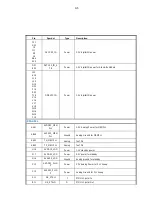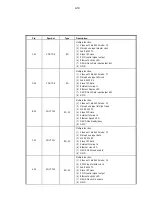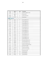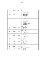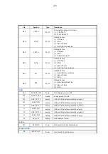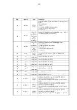
Pin Symbol Type
Description
E20
ʳ
UATXD
I/O, 5V
Reserved for debug-only Uart pins
(1) 1
st
RS232 TX
(2) T8032 RS232 TX
A22
ʳ
VCLK
I/O, 5V
Multiple function
(1) VFD clock
(2) GPIO
(3) Slave I2C data
(4) Serial interface data line
A23
ʳ
VDATA
I/O, 5V
Multiple function
(1) VFD data
(2) GPIO
(3) External Interrupt 3
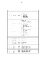
B23
ʳ
VSTB
I/O, 5V
Multiple function
(1) VFD strobe
(2) GPIO
(3) Slave I2C clock
(4) Serial interface control line
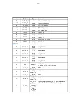
AA1
ʳ
SCL
I/O, 5V
Multiple function
(1) Serial interface control line
(2) Slave I2C clock
(3) GPIO
AA2
ʳ
SDA
I/O, 5V
Multiple function
(1) Serial interface data line
(2) Slave I2C data
(3) GPIO
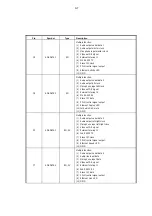
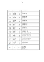
USB
AA3 AVDD33_USB Power
3.3V Analog power for USB
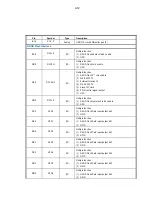
W4 AVSS33_USB
Ground
Analog ground for USB
W2 USB_DM_P0
Analog
USB port0 differential serial data bus (minus)
W1 USB_DP_P0
Analog
USB port0 differential serial data bus (plus)
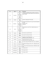
Y2 USB_DM_P1
Analog
USB port1 differential serial data bus (minus)
Y1 USB_DP_P1
Analog
USB port1 differential serial data bus (plus)
V2 USB_DM_P2
Analog
USB port2 differential serial data bus (minus)
V1 USB_DP_P2
Analog
USB port2 differential serial data bus (plus)
U3 USB_VRT
Analog
USB reference resistor
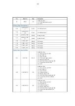
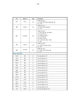
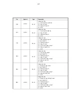
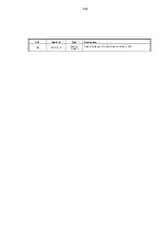
E-fuse
W7
ʳ
EFPWRQ
Power
2.5V power for E-fuse programming
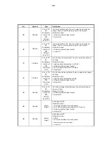
Ethernet PHY
G9 AVDD33_LD
Power
Line driver 3.3V analog power
9-19
Summary of Contents for BDP2105
Page 11: ...4 3 5 SOURCE 1 2 TV 2 4 ...
Page 12: ...6 USB DVD VCD CD BD BD 3D DivX Plus HD MKV MP3 JPEG 2 3 4 1 1 2 3 2 5 ...
Page 40: ...7 6 7 6 Front Board Print layout bottom side for BDP2180 12 05 ...
Page 41: ...7 7 7 7 Front Board Print layout bottom side for BDP2180X 78 ...
Page 42: ...7 8 7 8 Front Board Print layout bottom side for BDP2180X 78 ...
Page 43: ...7 9 7 9 Power Board Print layout bottom side for BDP2180 12 05 X78 ...
Page 46: ...PIN ASSIGNMENT 9 2 ...

