background image

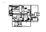
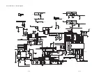
FLOW CHART NO.4

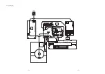
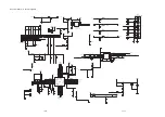
FLOW CHART NO.5

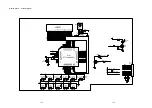
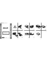
FLOW CHART NO.6

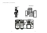
Pass in and out can not read dish sometime.

Can not read dish

Can not pass in and out 

Check dish if put on the right position or not.

Check pin connector location CN4 at decoder board  is loose or not

Check  cable locatio CN2 is loose or not

Check dish if cleanlily or not.

Yes

Troubleshooting

9-2

Summary of Contents for DCD322/12

Page 1: ... 2 4 Safety Check After Servicing 4 1 6 Standard Notes For Servicing Lead Free Requirements Handling Flat Pack IC 6 1 to 6 4 5 Safety Information General Notes Lead Free 7 Direction of Use 7 1 to 7 5 8 Cabinet Disassembly Instructions 8 1 to 8 2 12 AMP Board 9 Troubleshooting 9 1 to 9 2 10 Block Diagram 10 1 11 Wiring Diagram 11 1 13 Display Board 14 Headphone and USB Board Layout Diagram 12 5 15 ...

Page 2: ...Q RXWSXW G Audio Input Output COAXIAL Digital In DTS according IEC 61937 1 5 Connectivity Video In Output USB Compatibility USB2 0 Type of connector Series A Connector Class support UMS USB Mass Storage Class File System FAT12 FAT16 FAT32 Sampling Frequency MP3 22kHz 44 1kHz 48kHz WMA 44 1kHz 48kHz Canstant bit rate CVBS MP3 32 320 kbps Amplitude Output 1Vpp 10 White Bar 714mV 10 Sync Amplitude 28...

Page 3: ...W Picture CD USB Digital Camera PTP USB flash drive x 2 Picture Compression Format JPEG JPEG digital camera photos x 3 Picture enhancement Slideshow with MP3 playback Create albums Rotate Slideshow with music playback Zoom x 1 5 Dimension and Weight Main Unit WxHxD 223X88X242mm Net Weight 1 8kg Speaker Box WxHxD 140x220x220mm Net Weight 3 9kg Technical Specifications and Connection Facilities Type...

Page 4: ...the pickup lens when the diode is turned on Do not look directly at the laser beam CAUTION Use of controls and adjustments or doing procedures other than those specified herein may result in hazardous radiation exposure Location Inside Top of Blu Ray mechanism Do not look directly at the laser beam coming from the pickup or allow it to strike against your skin Drive Mechanism Assembly Laser Beam R...

Page 5: ...mpartment if you are not using the product for an extended period of time Only use microfiber cloth to clean the product Important Important Safety Precautions Read and understand all instructions before you use your home theater If damage is caused by failure to follow instructions the warranty does not apply Safety Riskof electricshockor re Never expose the product and accessories to rain or wat...

Page 6: ...ic products Please act according to your local rules and do not dispose of your old products with your normal household waste Correct disposal of your old product helps to prevent potential negative consequences for the environment and human health Your product contains batteries covered by the European Directive 2006 66 EC which cannot be disposed with normal household waste Please inform yoursel...

Page 7: ... and externally exposed accessible parts RF terminals antenna terminals video and audio input and output terminals microphone jacks earphone jacks etc is lower than or equal to the specified value in the table below Measuring Method Power ON Insert load Z between B earth ground power cord plug prongs and exposed accessible parts Use an AC voltmeter to measure across the terminals of load Z See Fig...

Page 8: ...e sure that during repair you are at the same potential as the mass of the set by a wristband with resistance Keep components and tools at this same potential Available ESD protection equipment Complete kit ESD3 small tablemat wristband 4822 310 10671 Wristband tester 4822 344 13999 Be careful during measurements in the live voltage section The primary side of the power supply including the heatsi...

Page 9: ...older paste is required please contact the manufacturer of your solder equipment In general use of solder paste within workshops should be avoided because paste is not easy to store and to handle Use only adequate solder tools applicable for lead free solder alloy The solder tool must be able To reach at least a solder temperature of 400 C To stabilize the adjusted temperature at the solder tip To...

Page 10: ... this and more technical information within the magazine chapter workshop news For additional questions please contact your local repair helpdesk How to Remove Install Flat Pack IC 1 Removal With Hot Air Flat Pack IC Desoldering Machine 1 Prepare the hot air flat pack IC desoldering machine then apply hot air to the Flat Pack IC about 5 to 6 seconds Fig S 1 1 2 Remove the flat pack IC with tweezer...

Page 11: ...e flat pack IC you can remove it easily Fig S 1 3 2 Affix the wire to a workbench or solid mounting point as shown in Fig S 1 5 3 While heating the pins using a fine tip soldering iron or hot air blower pull up the wire as the solder melts so as to lift the IC leads from the CBA contact pads as shown in Fig S 1 5 4 Bottom of the flat pack IC is fixed with glue to the CBA when removing entire flat ...

Page 12: ...lectrostatic charge during unpacking or repair work 1 Ground for Human Body Be sure to wear a grounding band 1 M that is properly grounded to remove any static electricity that may be charged on the body 2 Ground for Workbench Be sure to place a conductive sheet or copper plate with proper grounding 1 M on the workbench or other surface where the semi conductors are to be placed Because the static...

Page 13: ...ious next track title or chapter Select a preset radio station Start or pause play Stop play or erase a program MODE DIM Select repeat shufÀe play modes Select a brightness level for the display screen Open or close the disc compartment MP3 LINK Jack for an external audio device 1 1 2 3 4 5 6 7 8 9 10 11 12 13 14 15 16 17 1 2 3 4 18 19 20 21 22 23 2 3 4 5 6 7 8 9 1 2 3 4 5 6 7 8 9 10 11 12 13 10 1...

Page 14: ...he clock View the clock SLEEP TIMER Set the sleep timer Set the alarm timer SUBTITLE Select a subtitle language GOTO During disc play specify a position to start play ANGLE PROG Select a DVD camera angle Program tracks Program titles chapters for DVD play Program radio stations Numeric keypad Select a title chapter track directly Skip to the previous next track Skip to the previous next title or c...

Page 15: ... left speaker to L Connect FM antenna Tip For optimal reception fully extend and adjust the position of the antenna For better FM stereo reception connect an outdoor FM antenna to the FM AERIAL jack The unit does not support MW radio reception 1 Connect the supplied FM wire antenna to the FM AERIAL socket on the unit Spea ker Right Spea ker Left Connect audio cables To hear audio from other audio ...

Page 16: ...r a standard TV Option 1 Connect through an S Video cable 1 Connect an S video cable not supplied to the S Videosocket on this unit the S Videosocket on the TV TV S VIDEO IN S VIDEO Option 2 Connect through a composite video cable 1 Connect the composite video cable supplied to the VIDEO socket on this unit the video input socket on the TV Option 3 Connect through component video cables TV TV COMP...

Page 17: ... device optional You can also listen to an external audio device through this unit Option 1 Connect through the AUX IN sockets Option 2 Connect through the MP3 LINK socket TV Option 1 Connect through the AUX IN sockets 1 Connect audio cables red white to the AUX IN L andR sockets on this unit the audio output sockets on the external audio device Option 2 Connect through the MP3 LINK socket 1 Conne...

Page 18: ... CNxx Jxx CONxx Connector D3 5X12BA is specification of screw Unhook Unlock Release Unplug or Desolder e g 7 01 seven Screws ID Loc No Part Removal Fig No Remove Unhook Unlock Release Unplug Desolder Note 1 2 3 4 5 6 2 A02 D3x6KB 1 A03 D3x10FA 3 A04 D2x8BT 2 A01 D3x8KM 1 A05 D3x10FT 4 A08 D3x6PWTT 5 A05 D3x10FA 4 A07 D3x15FM 3 A04 D2x8BT 4 A04 D2x8BT 5 A09 D3x8PA D1 D2 D3 D4 D5 D6 PCB Bracket 4 A0...

Page 19: ...8 2 Cabinet Disassembly Instructions Fig D5 Fig D6 Fig D3 Fig D4 A06 A07 A05 A08 A04 A04 A09 ...

Page 20: ...02 pin 2 MUTE whether has high level If at low level state the MUTE function action test pin 3 STBY whether at low level Yes Yes Yes Yes No Yes Retry again Cancel the MUTE setup No Check replace MPEG board Test the location CN301 pin 2 4 whether has 19 and 5v provided voltage Replace a new AMP board Yes Yes No Check related electric circuit FLOW CHART NO 3 Do not display Check related electric cir...

Page 21: ...ot read dish sometime Can not read dish Can not pass in and out Check dish if put on the right position or not Check pin connector location CN4 at decoder board is loose or not Check cable locatio CN2 is loose or not Check dish if cleanlily or not Yes Troubleshooting 9 2 ...

Page 22: ...ONE MCU_MUTE STANDBY MCU_MUTE DM 06BXLX L2 Foryou pick up DVD Loader CLOSE DOOR OPEN DOOR MPEG_ON PT2309 5V STANDBY A12V 12V 5V 22V ECO_POWER A5V Ipod L R BD3491FS AUDIO PROCESSOR I2C_MPEG I2C_MAIN ECO_POWER A5V LCD_BUS LCD_BUS IR_MCU IR_MCU OR DAB MODULE FM SI4704or4705 MODULE FM_L R A5V 5V_FM Headphone Amp M5V 22V MUTE_AMP STANDBY MUTE BUFFER MCU_MUTE MCU_MUTE NEP040 050E MPEG_ON S_PO_MPEG OPTIO...

Page 23: ...5P 2 0 6P 2 0 IPOD BOARD Headphone USB Board CN301 GND DP DM 5V 4P 2 0 CN302 GND HP L HP R HP MUTE MP3 L GND MP3 R CN303 3P 2 0 4P 2 0 GND 5V IPOD VCC IPOD TX IPOD TR GND IPOD DET GND IPOD L IPOD R CN401 10P 2 0 GND 3P 2 0 J1 MP3 L MP3 R GND 5V IPOD VCC IPOD TX IPOD TR GND IPOD DET GND DP DM 5V REST MCLK J9 10P 1 25 MDA IR LED 5V GND GND AD1 AD2 CN1 4P 2 0 J2 5P 2 0 J11 2P 2 0 J5 3P 2 0 STBY MUTE ...

Page 24: ... 104 C139 102 C142 102 C135 224 C143 224 L IN R IN R1351M R1341M R136 30K C148 10UF 50V R123 0 R125 0 NC R126 0 R127 0 NC EC25 10UF 16v C130 104 C122 104 R26 5 6K R5 5 6K STBY MUTE VDDS C73 47P C111 47P C71 47P C72 47P C246 1uf 50v R218 1K R234 22K R113 1K R114 10K R111 47K R112 10K Q102 9014 Q103 9014 Q101 9014 5V L9 22UH 5A L8 22UH 5A C129 330p R130 20R C132 474 C128 224 C140 224 C119 330P C117 ...

Page 25: ...AMP Board Layout Diagram 12 2 12 2 ...

Page 26: ... seg15 seg16 seg17 seg18 seg19 seg20 seg2 LED seg4 LED102 LED 5V LED101 R105 10k R104 1 2K 5V R102 2 2K Q101 8550 R110 100 R113 47k ACC DET Q104 8050 R126 10 SEG15 36 SEG14 35 SEG13 34 COM4 17 COM3 16 SEG9 30 SEG0 21 SEG8 29 COM6 19 SEG6 27 SEG5 26 SEG4 25 SEG3 24 SEG2 23 SEG1 22 IRQ 9 OSCI 6 VDD 7 VLCD 8 SEG11 32 COM2 15 COM1 14 COM0 13 T3 12 T2 11 T1 10 COM7 20 COM5 18 SEG12 33 VSS 5 DATA 4 WR 3...

Page 27: ...Display Board Layout Diagram 12 4 12 4 ...

Page 28: ... Layout Diagram 1 2 3 4 CN202 4P 2 0 JA202A J1002C J1002B PGND H_OUTR H_OUTL PH MUTE R202 47K R201 47K C202 100P C201 100P vbus 1 D 2 D 3 GND 4 Shield 5 GND 6 JA203 DGND D D VBUS 1 2 3 4 CN203 4P 2 0 C205 100P C207 100P C206 100P Headphone Board USB Board Headphone Board USB Board 12 5 12 5 ...

Page 29: ...50 60Hz 1 2 CON1 CX2 0 1uF 275V R17 101R 1206 CE6 R9 5 1R2 1206 CE3 1000uF 10V 1000uF 10V CE9 1000uF 10V R1 R3 R12 R13 R11 CY2 471M 400V CY3 471M 400V Lp 0 56mH A Q2 882 TO 126 Q3 S8050 TO 92 TL431 IC4 A R31 10K 0805 R29 120R 2W R30 10K1 6W C L2 DR6 15 2uH R15 3R3 1206 D2 IN4007 CE2 47uF 50V 19 5V GND R32 9 1K 0805 C3 101 1kv R16 10K 1206 R14 10K 0805 R10 C15 102 1206 500V R25 120K 0805 5 2V GND C...

Page 30: ...05 R33 9 1K 0805 1 2 3 4 5 6 7 8 R36 IC5 T1 C C6 102pF 500V CE11 5 220uF 25V CE12 CE13 L3 10uH 0 6mm CE4 1000uF 25V CE10 C17 104 50V 0805 D10 SB240 C14 104pF 50V C7 104 50V 1 2 CON3 5 1V 1 0A GND CE4 MC34063A R39 150K 0805 C18 104 50V 1206 Power Board Circuit Diagram 2 12 7 12 7 ...

Page 31: ...Power Board Layout Diagram 12 8 12 8 ...

Page 32: ...t Right In Left In SGND Video Out NC NC GND Tx Rx NC GND GND NC 3 3V 12V 12V Serial enable TPA 5VDC TPA Data TPB Data TPB GND GND GND GND GND GND GND GND IP201 30P IP C404 104 TX RX R404 22K R405 22K IPOD AC IPOD AC C405 330P C406 330P C407 330P C408 330P C409 330P C413 330P LCH_IPOD RCH_IPOD TX RX IPOD_DET IPOD AC 5V 5V LCH_IPOD RCH_IPOD AGND IPOD_DET DGND video video 1 2 3 4 5 6 7 8 9 10 11 12 C...

Page 33: ...8 VDDQ DQ9 DQ10 VSSQ DQ11 DQ12 VDDQ DQ13 DQ14 VSSQ DQ15 VSS C29 10nF Y1 C2 22pF C7 22pF 27 000MHz U1 MX25L1605D 1 2 3 4 5 6 7 8 CS SO WP GND SI SCK HOLD VDD C3 10nF EC1 100uF 10V FB7 FB 2K C38 10nF C4 10nF C18 1nF R22 100R R4 15 4K 1 C1 10nF R156 75R1 C16 1nF C33 10nF FB11 MBW2012 221 EC6 100uF 10V R68 220R U2A ZR36966 102 101 93 92 91 90 86 84 87 85 82 83 81 88 89 70 80 72 76 77 74 75 71 68 69 73...

Page 34: ... TP3 C42 NM 470pF C50 0 1uF C61 0 1uF CN2 24Pin OPU connector 24 23 22 21 20 19 18 17 16 15 14 13 12 11 10 9 8 7 6 5 4 3 2 1 25 26 27 28 GND LD DVD LD NC HFM MD CD LD VR DVD VR CD NC E VCC VC VREF GND PD F B A RF CD DVD_SW D C T T F F GND GND GND GND EC8 220uF 6 3V TP21 EC9 220uF 6 3V C45 0 1uF Q5 SS8550 1 2 3 Q4 SS8550 1 2 3 R34 220R TP20 C52 1nF R55 1K 1 C56 33pF C54 27nF TP12 R112 2 2K R40 NM 9...

Page 35: ...9 1V 1 2 FB54 MBW2012 1K C154 2 2uF FB16 FB 2K C176 2 2uF U14 LM324 SO 14 NS 1 2 3 4 5 6 7 8 9 10 11 12 13 14 1OUT 1IN 1IN VDD 2IN 2IN 2OUT 3OUT 3IN 3IN GND 4IN 4IN 4OUT CB113 0 1uF R323 1K R90 100K D7 1N4148 1 2 C88 0 1u R177 47K EC29 220uF 16V C116 1uF FB49 MBW2012 1K C178 2 2uF R324 1K C153 2 2uF R354 8 2K FB53 MBW2012 1K R84 47K U6A CF4558 3 2 1 8 4 R133 22R1 4W 1 2 D17 1N4148 D15 1N4148 C177 ...

Page 36: ...R126 1K R121 1K EC25 47uF 16V R69 8 2K R70 11K EC24 47uF 16V R129 100R 1W C21 0 1uF C421 150pF C130 100pF R103 47K FB406 1K C101 1uF Q10 AO3407 R430 82R Q18 3904 1 2 3 R138 4 7K R159 1K R63 11K R139 10K R148 10K C423 150pF R149 4 7K R150 10K D13 1N4148 C75 1uF Q13 8050 1 2 3 Q14 3904 1 2 3 FB407 1K C139 0 1uF D12 3 9V 1 2 J7 CONN PCB 4 J_2 1 2 EC36 10u 16V C123 ESD5Z5C R140 1K C410 22pF EC26 47uF ...

Page 37: ...Decoder Board Layout Diagram 12 14 12 14 ...

Page 38: ...Exploded View PCB6 PCB4 PCB5 PCB2 18 23 23 23 23 15 PCB7 12 21 DVDM PCB1 17 14 16 13 LCD101 22 20 19 PCB3 11 13 1 13 1 ...

Page 39: ...Revision List Revision List Version 1 0 Initial Release 14 1 ...

Reviews: