Circuit Descriptions, List of Abbreviations, and IC Data Sheets
EN 81
DPTV565 AA
9.
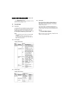
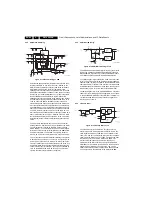
In Standby, the-5 volt Standby voltage is the only voltage being
applied to the set. The +15, +9, and +5.2 Volt sources are
turned "off". When the set is turned "on", the Standby Line goes
Low, turning transistor 7214 "off", turning 7205 "on", which
turns 7215 "on". This switches the +15 Volt supply to the set.
The +15 Volt supply then switches transistors 7216 and 7217
"on" to switch the +9 Volt and +5.2 Volt supplies to the set.
When the +15UV (Under Voltage detection) line goes "high",
transistor 7220 will turn "on", which will turn 7205 "off". This will
cause 7215 to turn "off", switching the +15, the +9, and the +5.2
Volt supplies "off". This will cause the set to shut down.
When troubleshooting, check for the presence of the operating
voltage on pin 7 of 7218. This 160 volts if the applied voltage is
120 volts AC or 328 volts is then applied voltage is 230 Volts
AC. If the Feedback circuit is not working or the secondary is
overloaded, pin 7 will be pulsing. In this case, check the voltage
on pin 5 of 7213. This is the operating voltage for pin 1 of 7218.
Each time the 5VSTBY voltage reaches 5 Volts, 7212 should
turn "on". The feedback opto isolator 7213 can be checked by
applying 5 volts to the +5VSTBY line with AC power removed
from the set. Vary the 5- volt supply between 4 and 6 Volts
while checking the resistance between Pins 4 and 5 of 7213.
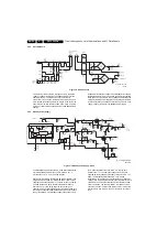
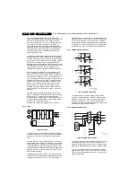
Under voltage Detection
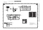
Figure 9-4 Under voltage detection circuit
If the 15-Volt supply drops below 11.2 Volts, transistor 7221 will
turn "off". The 5-Volt standby supply will be applied to the base
of 7220 (Figure " Standby power supply circuit") via resistors
3262 and 3263. This will cause the +15UV line to go "high". In
the Standby mode, the Standby line is "high" turning transistor
7222 "on". When the set is turned "on", 7222 turns "off".
Capacitor 2296 provides a delay to prevent the +15UV line
from going "high" before the +15V supply turns "on".
This circuit can be defeated by grounding the base of transistor
7220. When repairs are complete, this jumper should be
removed.
9.2.4
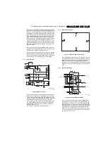
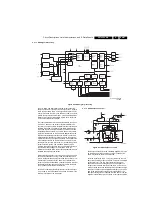
Main Power Supply
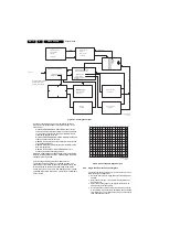
Figure 9-5 Main power supply circuit
The Main Power supply is located on the Large Signal panel.
The Main B+ voltage from the Input panel is applied to the Main
Power switching transistor, 7301, via Pins 6 and 8 of
transformer 5300. This voltage is protected by fuse 1300 and
filtered by choke 5330. The Standby line goes "low" when the
set is turned "on". Transistor 7309 is turned "off", which turns
7300 "on". This turns relay 1305 "on". The Start-up voltage is
applied to capacitor 2303 via resistor 3300. When 2303
charges to 14.5 Volts, the under-voltage lockout of 7302
connected to pin 1 is turned "on". Drive is output on pin 3 to the
switching FET, 7301. This signal drives 5300 to produce the
Main Power supply voltages. IC 7302 will continue to drive
5300 until the charges on capacitor 2303 drop below 9.4 Volts.
The Under voltage Lockout of 7302 will then turn the output on
pin 3 "off" until 2303 again charges to 14.5 Volts. After several
start-up cycles, the operating voltage for 7302 is supplied by
pin 10 of 5300.
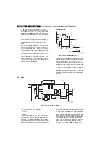
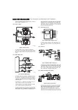
Regulation is accomplished by monitoring the 130V_S supply
via resistors 3324, 3350, 3323, and 3322. The feedback
voltage is applied to the Shunt Regulator 7304, which drives
the feedback opto-isolator 7303. The feedback voltage is
applied to pin 14 of 7302. The voltage is fed to comparator "C"
which is referenced to 2.5 Volts. This output of this comparator
E_15000_069.eps
151004
E_15000_070.eps
151004


