background image

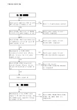
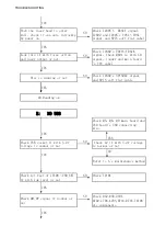
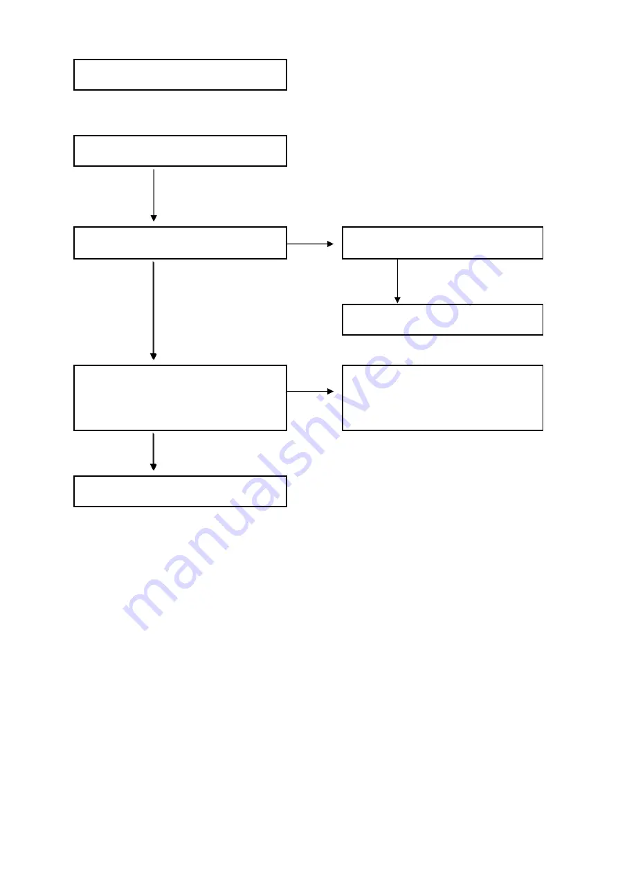
NO

YES

YES

NO

YES

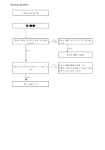
F: NO BT

USB reading OK

BT connect ok

Check RX TX waveform is normal or

not

Check R004,R005,CP001 or
CN001,IC111(on Main board),and
16PIN soft flat cable

Check D001 is with 3.3V voltage

or not

Check Q001 is with 3.3V voltage
or not

Check Q001,Q002

TROUBLE SHOOTING

Summary of Contents for DTM5096

Page 1: ...DTM5096 Version 2 0 wk1505 ...

Page 2: ...USB Board AUDIO IN Board Location of PC Boards Main Board CD Board BT Board BT LED Board Key Board 1 Location of PC Boards Versions Variation ...

Page 3: ...C Boards Versiongs Variation FM ANT Board SMPS Board Tips C Component Level Repair M Module Level Rpair CD Board SMPS Board Main Board KEY Board FM ANT Board AUIDO IN Board BT LED Board BT Board USB Board Type Version Board in used service Policy DTM5096 12 EU 12 APMEA ...

Page 4: ...eo Off pont dbuV Channel separation 400 1000 5000Hz 声道分不平衡 Channel unbalance 250 to 6300Hz 250 to 6300Hz 25 停震电压 V N A N A Osc stop voltage V N A N A kHz Frequency drift vs temp kHz kHz 27 选台灵敏度 Search tuning sensitivity dBuV 16 to 28 11 to 35 32 34 35 32 34 35 FM 电气指标及数据 MODEL DTM5096 标准输出Ref o p 500 mW 负载O P imped R L LS 6 ohm Woofer 6 ohm 供电电压Supply see version table 条件 Condition 40kHz dev 14 5...

Page 5: ...衡 Channel balance dB 0 2 0 2 0 2 dB 0 2 N A N A 负载O P imped R L LS 6 ohm Woofer 6 ohm 标准输出Ref o p 500 mW 标准输出Ref o p 500 mW 负载O P imped R L LS 6 ohm Woofer 6 ohm 9 10 N A N A N A 29 87 5 to 108MHz S 60 time of total tuning range 选台总时间 65 81to74 87 5to108MHz 100 1mV 75kHz dev For reference only N A min max vol Refer to sh190 40kHz dev 1 5 条件 Condition FRONT R L 3 1 LIVING SOUND 2 FRONT R L LIVING S...

Page 6: ...32 30 30 W 20 16 10 10 W 70 56 62 63 dB 80 75 88 88 dB 62 57 87 87 dB 62 57 80 80 噪声 最大音量 20dB Hum mV 1 3 0 6 0 6 4 2 6 7 5 信噪比 S N wtd DBA 标准输出Ref o p 500 mW 负载O P imped R L LS 6 ohm Woofer 6 ohm 10 THD output power 500MV 10 失真输出 音频Audio part Input 1KHZ 500mv test signal copy from Audio Signal 1 disc SBC429 data 10 9 5 3 osstalk 1K 2 FRONT R L LIVING SOUND SUB WOOFER FRONT R L LIVING SOUND 4 FRON...

Page 7: ...dB hum mV 1 3 0 5 0 5 mV 1 3 0 6 0 6 mV 1 3 0 5 0 5 mv 0 6 0 8 0 2 0 2 mv 0 6 0 8 0 1 0 1 mv 0 6 0 8 0 1 0 1 8 2 电平比较 Level Matching 9 音频Audio part test signal copy from Audio Signal 1 disc SBC429 data setting will be TBC I PHONE IPOD I PHONE 5 電氣指標及數據 I PHONE 5 Electrical Specification Data 信噪比 SNR wtd DBA 10 Min volume residual noise 最小音量 残余 噪声 标准输出Ref o p 500 mW 负载O P imped R L LS 6 ohm Woofer ...

Page 8: ... 3 0 5 0 5 mV 1 3 0 6 0 6 mV 1 3 0 6 0 6 最小音量 残余 噪声 mv 0 6 0 8 0 1 0 1 mv 0 6 0 8 0 2 0 2 mv 0 6 0 8 0 2 0 2 11 最大输出电平 Max output V N A N A BT Electrical Specification Data BLUE TOOTH 電氣指標及數據 9 10 1 Min volume residual noise 5 3 供电电压Supply see version table 2 标准输出Ref o p 500 mW 负载O P imped R L LS 6 ohm Woofer 6 ohm For reference only 20db 0dB 条件 Condition FRONT R L 音频Audio part test signal copy fr...

Page 9: ... cord and connect a wire between the two pins of the mains plug 2 Set the mains switch the on position keep the mains cord unplug 3 Measure the resistance value between the mains plug and the front panel controls and chassis bottom 4 Repair or correct unit when the resistance measurement is less than 1M 5 Verify this before you return the unit to the customer user ref UL standard no 1492 6 Switch ...

Page 10: ...Commutate Filter u1 x2 x1 f x1 xn AMP_30V 5A 6 5V 1 5A 3 5V 0 3A 28V 0 3A GND AMP_GND Power Ctrl Standby 5 2V 2 1A ...

Page 11: ...r Amplifier STA326 30Wx2ch PERSET EQ VOLUNE Power Amplifier STA326 30W 70W DSP CS48540 Switch ADC CE2631 DM DP L R C SW IR Receiver VFD Display VFD20 1033 Touch Key x 10 GT1000A USB Audio System CPU OTK5250 16M SDRAM VFD Driver ET16315 SPI Flash GD25Q80 32 768KHz 24MHZ 16 93MHZ ...

Page 12: ...5 Set Wiring Diagram ...

Page 13: ...6 DISMANTLING DIAGRAM 1 Dismantling of the top cabinet a Remove 8 screws A B as indicated to loosen the back cabinet A B ...

Page 14: ...b Remove 2 screws C as indicated to loosen the top cabinet C ...

Page 15: ...c Remove 8 screws D E F as indicated to loosen the top cabinet D E F ...

Page 16: ...tling the PCB board of the top a Remove 3 screws G as indicated to loosen the BT board b Remove 4 screws H as indicated to loosen the Key board c Remove 2 screws I as indicated to loosen the BT LED board G I H ...

Page 17: ...d Remove 4 screws J as indicated to loosen the Main board e Remove 3 screws K as indicated to loosen the CD board J K ...

Page 18: ...f Remove 1 screws L as indicated to loosen the USB AUDIO IN board g Remove 2 screws M as indicated to loosen the IR board L M ...

Page 19: ...3 Dismantling of the bottom cabinet 1 Remove 10 screws O P as indicated to loosen the back cabinet O P ...

Page 20: ...b Remove 2 screws R as indicated to loosen the FM ANT board a Remove 4 screws Q as indicated to loosen the SMPS board 2 Dismantling the PCB board of the Bottom R Q ...

Page 21: ...7 1 Main Board Circuit Diagram ...

Page 22: ...Main Board Circuit Diagram ...

Page 23: ...Main Board Circuit Diagram ...

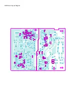
Page 24: ...7 2 Main Board Layout Diagram ...

Page 25: ...Main Board Layout Diagram ...

Page 26: ...Main Board Layout Diagram ...

Page 27: ...Main Board Layout Diagram ...

Page 28: ...Main Board Layout Diagram ...

Page 29: ...Main Board Layout Diagram ...

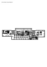
Page 30: ...BT Board Layout Diagram ...

Page 31: ...BT Board Layout Diagram ...

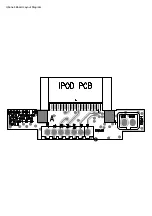
Page 32: ...Iphone4 Board Layout Diagram ...

Page 33: ...Iphone4 Board Layout Diagram ...

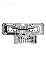
Page 34: ...Iphone5 Board Layout Diagram ...

Page 35: ...Iphone5 Board Layout Diagram ...

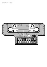
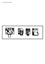
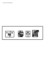
Page 36: ...Input Board Layout Diagram ...

Page 37: ...Input Board Layout Diagram ...

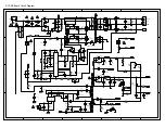
Page 38: ... 250V 30V D19 1N4148 GND R44 5 1K C65 103 DW2 15V 0 5W 30V HV TR3 U1B 817 C36 1000u 16V 5 2V GND L2 RB2 330R RB3 510R RB5 10K 1 IC4 431 C24 104 RB4 9 1K 1 GND P down D25 SB560 C34 102 C35 1000u 16V RB18 51R RA4 4 7R D4 HER107 D20 HER007 RS1 RS2 2R HV C19 10uF 50V RA6 10R C38 104 30V 5VSB RB13 5 1K D22 HER107 C30 4 7uF 50V RA5 470R T1 RA8 U2A 817 GND D2 FR107 U2B 817 RB7 330R T3 1815 RB12 5 1K PSON...

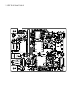
Page 39: ...8 2 SMP Board Layout Diagram ...

Page 40: ...SMP Board Layout Diagram ...

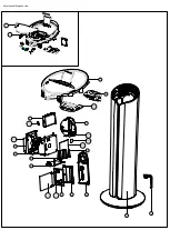
Page 41: ...9 Mechanical Exploded View ...

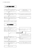
Page 42: ...or not B NO DISPLAY Check D25 D27 IC4 U1 Check D703 D704 D705 VFD display drive signal CLK DATE STB is normal or not Check IC101 CN5 and on display board IC701 CN702 FFC cabel Check X101 X102 R48 R55 R47 C23 etc components A NO POWER OUTPUT CheckRS1 RS2 C18 D20 D21 TR3 Check the fourth feet of IC2 is with around 14V is normal or not Check RA4 D4 TR3 IC4 Check C12 is with 310V direct voltage is nor...

Page 43: ... with 3 3V power supply or not Check power supply circuit L7 L46 L52 L30 IC2 component C NO SOUND Check power amplifier DD1 if with 30V voltage is normal or not Refer to A maintenance method Measurement of the IC601 power supply 3 3V and 1 8V voltage and the IC602 power supply5V voltage is normal or not Check IC203 24pin and 42pin feet of CS48540 is with 3 3V and 1 8V power supply or not Check pow...

Page 44: ...s action and laser output or not Disc is running or not Check IC602 s SPINDLE signal and 6PIN soft flat cable CD Reading ok Check DM DP signal if normal or not Check R52 R58 D701 D702 L704 L705 R744 R745 IC108 etc components Check IC602 s FOCUS TRACK signal Check Q601 is with LD signal loader and main board s FFC cabel Check USB socket if with 5 2V voltage is normal or not Check L2 if with 5 2V vo...

Page 45: ...K BT connect ok Check RX TX waveform is normal or not Check R004 R005 CP001 or CN001 IC111 on Main board and 16PIN soft flat cable Check D001 is with 3 3V voltage or not Check Q001 is with 3 3V voltage or not Check Q001 Q002 TROUBLE SHOOTING ...

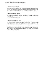
Page 46: ...1 3 How to upgrade the software Copy the upgrade files System files include upgrade txt and upgrade_dcm5090 bin into USB plug the USB into products display will show UPGRADE which means it is getting upgrade After dozens of second display will show SUCCESS which means the upgrade is done Then can plug up the power cable and remove the USB Please pay attention that it must not blackout while upgrad...

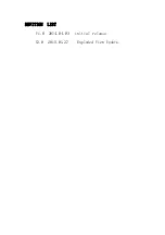
Page 47: ...REVITION LIST V1 0 2014 04 03 initial release V2 0 2015 01 27 Exploded View Update ...

Reviews: