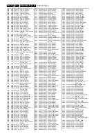
Circuit-, IC Descriptions and List of Abbreviations
GB 296
DVDR1000 /0x1 /691
9.
Pin Connections and Functions
Pin #
Name
Description
Power Supply Connections (not shown on Block diagram)
See list
V
SS
Ground connections. Connect to the digital ground plane. Pins: 2, 17, 34, 55, 64, 74, 85,
96, 106, 115, 124, 132, 138, 145, 152, 159, 168
See list
V
DD33
Pad Ring digital power connections. Connect to the digital 3.3 volt power supply and
decouple to the digital ground plane. Pins: 1, 33, 63, 73, 84, 95, 105, 114, 123, 137, 144,
151, 167
See list
V
DD25
Core Logic digital power connections. Connect to the digital 2.5 volt power supply and
decouple to the digital ground plane. Pins: 16, 54, 107, 158
43
AV
SS
Ground connection for the clock PLL circuits. Connect to the digital ground plane
42
AV
DD
Analog power connections for the clock PLL circuit. Connect to a separately decoupled 2.5
volt power supply and decouple directly to the AV
SS
pin..
Control Signals
49
RESETB
Reset. When this input is set low it will reset all the internal registers to the default states.
Refer to the section on the control registers for details of these states. The device must be
reset after it is powered-up.
53
OE
When this pin is set high the outputs of the FLI2200 will be enabled; when it is set low the
outputs will be set into a high-impedance state.
56-58
IFORMAT
2-0
Input signal format control. The settings of these pins set the format of the input signal.
This can be overridden by the IFmtOvr bit, bit 3 in register 00
H
, allowing this function to be
set or changed via the I
2
C bus. Please refer to the description of register 00
H
for details.
59-61
OFORMAT
2-0
Output signal format control. The settings of these pins set the format of the output signal.
This can be overridden by the OFmtOvr bit, bit 3 in register 07
H
, allowing this function to be
set or changed via the I
2
C bus. Please refer to the description of register 07
H
for details.
44-45
DADDR
1-0
The settings of DADDR
1-0
allow the device address of the control bus to be programmed to
prevent conflict with the other devices connected to the bus. DADDR
1-0
allow the device
address to be set to any of the following values: C0/C1
H
, C2/C3
H
, E0/E1
H
, E2/E3
H
. Please refer
to the section “Control Bus Operation and Protocol” for further information.
46
MODE
When this pin is set low the control bus will operate in the slave mode; allowing the device to
programmed from an external controller. When it is set high the FLI2200 will self-program from
an external I
2
C memory connected to the bus. Please refer to the “Control Bus Operation and
Control Protocol” section for more details.
47
SDA
2-wire serial control bus data. Data can be written to the control registers via this pin when it
is in the input mode and data can be read from the status registers when it is in the output
mode. Refer to the section on the serial port for timing and format details and to the section on
the registers for programming information.
48
SCL
2-wire serial control bus clock. When the control port operates in slave mode this pin will be
an input and when it operates in the self programming mode it will be an output.
40
PIXCLK
Pixel clock input. This clock is used to drive all the circuits in the FLI2200. An internal PLL is
used to upconvert this clock to provide the master clock signal and other clocks used
internally. Note that when the FLI2200 is used in the D1 input mode the PIXCLK input
should run at the rate of two cycles per pixel (one for luma and one for chroma).
62
N/P/IN/OUT
NTSC/PAL input or output. The default function of this pin is NTSC/PAL signal indicator
output. When the input video signal is a 525 line signal this pin will be set high and when it
is a 625 line signal the pin is set low. This function of this pin can be programmed to be an
input according to the setting of this pin if the NPOp
1-0
bits, bits 5-4 in register 03
H
, are set
to 00
H
, overriding the internal line counter. i.e., it will treat the signal as a 525 line signal
when it is set high and a 625 line signal when it is set low.
Summary of Contents for DVDR1000/001
Page 10: ...Directions For Use GB 10 DVDR1000 0x1 691 3 ...
Page 12: ...Directions For Use GB 12 DVDR1000 0x1 691 3 ...
Page 13: ...Directions For Use GB 13 DVDR1000 0x1 691 3 ...
Page 14: ...Directions For Use GB 14 DVDR1000 0x1 691 3 ...
Page 16: ...Directions For Use GB 16 DVDR1000 0x1 691 3 ...
Page 17: ...Directions For Use GB 17 DVDR1000 0x1 691 3 ...
Page 19: ...Directions For Use GB 19 DVDR1000 0x1 691 3 ...
Page 27: ...Directions For Use GB 27 DVDR1000 0x1 691 3 ...
Page 30: ...Directions For Use GB 30 DVDR1000 0x1 691 3 ...
Page 31: ...Directions For Use GB 31 DVDR1000 0x1 691 3 ...
Page 90: ...Diagnostic Software and Faultfinding Trees GB 90 DVDR1000 0x1 691 5 Personal Notes ...
Page 183: ...Circuit IC Descriptions and List of Abbreviations GB 183 DVDR1000 0x1 691 9 ...
Page 184: ...Circuit IC Descriptions and List of Abbreviations GB 184 DVDR1000 0x1 691 9 ...
Page 185: ...Circuit IC Descriptions and List of Abbreviations GB 185 DVDR1000 0x1 691 9 ...
Page 194: ...Circuit IC Descriptions and List of Abbreviations GB 194 DVDR1000 0x1 691 9 ...
Page 195: ...Circuit IC Descriptions and List of Abbreviations GB 195 DVDR1000 0x1 691 9 ...
Page 196: ...Circuit IC Descriptions and List of Abbreviations GB 196 DVDR1000 0x1 691 9 ...
Page 197: ...Circuit IC Descriptions and List of Abbreviations GB 197 DVDR1000 0x1 691 9 ...
Page 198: ...Circuit IC Descriptions and List of Abbreviations GB 198 DVDR1000 0x1 691 9 ...
Page 199: ...Circuit IC Descriptions and List of Abbreviations GB 199 DVDR1000 0x1 691 9 ...
Page 200: ...Circuit IC Descriptions and List of Abbreviations GB 200 DVDR1000 0x1 691 9 ...
Page 201: ...Circuit IC Descriptions and List of Abbreviations GB 201 DVDR1000 0x1 691 9 ...
Page 202: ...Circuit IC Descriptions and List of Abbreviations GB 202 DVDR1000 0x1 691 9 ...
Page 204: ...Circuit IC Descriptions and List of Abbreviations GB 204 DVDR1000 0x1 691 9 ...
Page 205: ...Circuit IC Descriptions and List of Abbreviations GB 205 DVDR1000 0x1 691 9 ...
Page 206: ...Circuit IC Descriptions and List of Abbreviations GB 206 DVDR1000 0x1 691 9 ...
Page 207: ...Circuit IC Descriptions and List of Abbreviations GB 207 DVDR1000 0x1 691 9 ...
Page 209: ...Circuit IC Descriptions and List of Abbreviations GB 209 DVDR1000 0x1 691 9 ...
Page 210: ...Circuit IC Descriptions and List of Abbreviations GB 210 DVDR1000 0x1 691 9 ...
Page 211: ...Circuit IC Descriptions and List of Abbreviations GB 211 DVDR1000 0x1 691 9 ...
Page 212: ...Circuit IC Descriptions and List of Abbreviations GB 212 DVDR1000 0x1 691 9 ...
Page 213: ...Circuit IC Descriptions and List of Abbreviations GB 213 DVDR1000 0x1 691 9 ...
Page 214: ...Circuit IC Descriptions and List of Abbreviations GB 214 DVDR1000 0x1 691 9 ...
Page 215: ...Circuit IC Descriptions and List of Abbreviations GB 215 DVDR1000 0x1 691 9 ...
Page 216: ...Circuit IC Descriptions and List of Abbreviations GB 216 DVDR1000 0x1 691 9 ...
Page 222: ...Circuit IC Descriptions and List of Abbreviations GB 222 DVDR1000 0x1 691 9 ...
Page 223: ...Circuit IC Descriptions and List of Abbreviations GB 223 DVDR1000 0x1 691 9 ...
Page 224: ...Circuit IC Descriptions and List of Abbreviations GB 224 DVDR1000 0x1 691 9 ...
Page 264: ...Circuit IC Descriptions and List of Abbreviations GB 264 DVDR1000 0x1 691 9 ...
Page 265: ...Circuit IC Descriptions and List of Abbreviations GB 265 DVDR1000 0x1 691 9 ...
Page 266: ...Circuit IC Descriptions and List of Abbreviations GB 266 DVDR1000 0x1 691 9 ...
Page 269: ...Circuit IC Descriptions and List of Abbreviations GB 269 DVDR1000 0x1 691 9 ...
Page 270: ...Circuit IC Descriptions and List of Abbreviations GB 270 DVDR1000 0x1 691 9 ...
Page 271: ...Circuit IC Descriptions and List of Abbreviations GB 271 DVDR1000 0x1 691 9 ...
Page 273: ...Circuit IC Descriptions and List of Abbreviations GB 273 DVDR1000 0x1 691 9 ...
Page 274: ...Circuit IC Descriptions and List of Abbreviations GB 274 DVDR1000 0x1 691 9 ...
Page 283: ...Circuit IC Descriptions and List of Abbreviations GB 283 DVDR1000 0x1 691 9 ...
Page 284: ...Circuit IC Descriptions and List of Abbreviations GB 284 DVDR1000 0x1 691 9 ...
Page 285: ...Circuit IC Descriptions and List of Abbreviations GB 285 DVDR1000 0x1 691 9 ...
Page 286: ...Circuit IC Descriptions and List of Abbreviations GB 286 DVDR1000 0x1 691 9 ...
Page 288: ...Circuit IC Descriptions and List of Abbreviations GB 288 DVDR1000 0x1 691 9 ...
Page 289: ...Circuit IC Descriptions and List of Abbreviations GB 289 DVDR1000 0x1 691 9 ...
Page 290: ...Circuit IC Descriptions and List of Abbreviations GB 290 DVDR1000 0x1 691 9 ...
Page 291: ...Circuit IC Descriptions and List of Abbreviations GB 291 DVDR1000 0x1 691 9 ...
Page 292: ...Circuit IC Descriptions and List of Abbreviations GB 292 DVDR1000 0x1 691 9 ...
Page 293: ...Circuit IC Descriptions and List of Abbreviations GB 293 DVDR1000 0x1 691 9 ...
Page 302: ...Circuit IC Descriptions and List of Abbreviations GB 302 DVDR1000 0x1 691 9 µ ...


