Circuit-, IC Descriptions and List of Abbreviations
EN 154
DVDR880-890 /0X1
9.
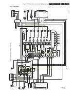
The processing of audio is always done in stereo (e.g. separate
left- and right-channel) and the complete switching is realized
by using HEF4052, which is a dual four-to-one multiplexer. In
principle there are three independent selectors:
a) Scart 1-Output-Path:
Pos [7504] is used to select either Scart 2-Input (“AIN2L”/
”AIN2R”) or the signal directly from the audio DAC [7001]
(“ALDAC”/”ARDAC”) as the output source for Scart 1
(“AOUT1L”/”AOUT1R”).
The control is done by means of the lines “ASC1S” coming from
[7408] (IC [7408] acts as a port expander for the CC-µP) and
“IASC1M”, which is directly coming from the CC. Pos [7412] is
used for level adaptation (3V3 to 5V) in between.
b) Scart 2-Output-Path:
Pos [7503] selects between Scart 1-Input (“AIN1L”/”AIN1R”),
signals from the internal frontend (“AFEL”/”AFER”) via MSP
[7600] or audio directly from the DAC [7001] (“ALDAC”/
”ARDAC”). The outputs of this switch are routed to Scart 2
(“AOUT2L”/AOUT2R”). This switch is controlled via “VSA1”-
and “VSA2”-line. These lines come from [7408] that is acting as
a port expander for the CC-µP.
c) Record-Path:
Pos [7501] selects either signals from Scart 1 (“AIN1L”/
”AIN1R”) or Scart 2 (“AIN2L”/”AIN2R”) or Cinch-Front (“AINFL”/
”AINFR”) or the MSP [7600] (“AFEL”/”AFER”) and routes to the
audio ADC [7005] (“ALADC”/”ARADC”) for record purposes.
The switch is controlled via “RSA1”- and “RSA2”-signals.
These signals come from the MSP [7600], which acts as a port
expander of the CC-µP. As there can also exist a fifth input in
case of DV-In is present the corresponding analog audio
signals from the DVIO-board are firstly routed via extra cable
and connector [1960] to the MSP. The MSP acts as a
preselector between audio from internal frontend or the DV-
Input.
Each of these three selectors ([7501], [7503] & [7504]) has a
separate Op-Amp on the output for level-adaptation-,
performance- and line-driving-reasons. [7505-A & -B] for
record, [7502-C & -D] for Scart 1-Output and [7502-A & -B]
respectively for Scart 2. Every audio output line on the two
Scart connectors can be “killed” (muted) by a extra transistors
([7506], [7508], [7509] &[7511]), which can be activated by the
“AKILL”-line. This signal is generated by the circuit around
[7404]/[7421] and is a combination of the “KILL”- from the CC-
µP and the “IPFAIL” of the power-supply-unit.
Additionally to analog audio the set is also equipped with a
digital output via cinch plug [1951]. The signal is generated on
the dig. board and routed via audio interface cable and
connector [1900] to the Ana-PCB. Here the “DAOUT”-line first
passes a 6-fold inverter [7580] being used as a driver and for
performance reasons (noise reduction, jitter, …). Afterwards a
transformer [5580] is necessary to achieve the correct level
and also to have a floating output with isolated ground before
the signal is fed via [3580] to cinch plug [1951]. The capacitor
[2580] performs an AC-coupling between connector- and set-
ground.
9.3.5
Audio ADC/DAC
The conversion of analog audio signals from the record-
selector [7501] in the I/O (“ALADC”- & “ARADC”) is done via
UDA1361TS [7005]. This IC can process input signals up to
2V
rms
by using external resistors [3039], [3041] in series to the
input pins. As the level from the DVIO-Board is only 1V
rms
a
6dB step can be performed by setting pin 7 of [7005] to 3,3V
via [7006] and the “PWONSW”-line controlled by the CC-µP to
use the whole dynamic range of the ADC. All required clock
signals are generated on the dig. board and only the audio
data (“A_DAT”-line) are routed from Ana- to Dig.-PCB for
further processing.
The transformation of dig. audio back into the analog domain
is done by UDA1334BTS [7001]. All necessary clock signals
are coming from the dig. board and dig. audio data
(“D_DATA0”-line) are converted into analog signals, which are
available at pin 14 and pin 16 of [7001]. Afterwards an Op-
Amp. [7002] (line driver & level adaptation) and a low-pass-fil-
ter to increase signal performance (noise, distortions,…). is
passed. Then both signals (“ALDAC” & “ARDAC”) are directly
routed to the rear cinch output and also used in the audio-I/O
for further processing. The DAC has also a mute possibility,
which can be activated by setting pin 8 to 3,3V via [7003]. This
mute is controlled either by the dig. board (“D_IKLL”-line) or
the “IPFAIL”-signal from power-supply-unit.
In addition to that the DAC [7001] and the cinch outputs can be
killed (muted) in case of “digital silence” by the circuit around
[7008],[7009] and [7010], when no audio data are available
(e.g. “D_DATA0”-line zero).
This function can be also activated via the “ION”-line (set to
high during any stand-by mode). To avoid signal distortions
(clipping) the mute transistors for cinch rear out [7415], [7416]
are decoupled via [7011].
Summary of Contents for DVDR880/001
Page 48: ...Mechanical Instructions EN 50 DVDR880 890 0X1 4 4 5 Dismantling Instructions Figure 4 14 ...
Page 166: ...Circuit IC Descriptions and List of Abbreviations EN 168 DVDR880 890 0X1 9 ...
Page 167: ...Circuit IC Descriptions and List of Abbreviations EN 169 DVDR880 890 0X1 9 ...
Page 174: ...Circuit IC Descriptions and List of Abbreviations EN 176 DVDR880 890 0X1 9 IC7411 ...
Page 182: ...Circuit IC Descriptions and List of Abbreviations EN 184 DVDR880 890 0X1 9 ...
Page 183: ...Circuit IC Descriptions and List of Abbreviations EN 185 DVDR880 890 0X1 9 ...
Page 184: ...Circuit IC Descriptions and List of Abbreviations EN 186 DVDR880 890 0X1 9 ...
Page 203: ...Circuit IC Descriptions and List of Abbreviations EN 205 DVDR880 890 0X1 9 ...

