Circuit-, IC Descriptions and List of Abbreviations
EN 156
DVDR880-890 /0X1
9.
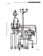
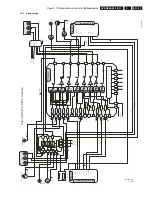
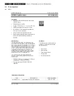
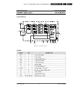
The complete Video-I/O-switching is basically realized by the
matrix switch STV6618 [7408], which is controlled via I²C-bus
by the CC. All used outputs excluding pin 21 (Y/CVBS-REC)
have a 6 dB-amplification and a 75 Ohms driver-stage inside.
This IC includes also several digital outputs, which are used for
switching purposes on the analog board. The record selector
inside the switch selects between the CVBS from frontend
(“VFV”), the input from Scart 1 (“YCVBSIN1”) or the signal from
Scart 2 (“YCVBSIN2”). Afterwards the signal passes another
switch [7411] in which a selection between signals from the
front or the preselected ones are done. The output signals of
[7411] are fed as “A_YCVBS”- and “A_C”-line to the digital
board for further processing.
To reduce the number of external presets there exists only one
preset for CVBS- and Y/C-front. The set automatically detects
between the two inputs depending on the presence of a video
signal (sync separator-circuit on mP-sub-board) where Y/C has
higher priority.
The R/G/B-inputs and the Fast-Blanking-line from Scart 2 are
directly routed to the digital PCB. These signals are also
available on the corresponding input-pins of the STV6618 to
enable a loop-through in AV-Standby. In this mode the set has
to behave like a cable between the two Scart-connectors. AV-
Standby is activated either by a “high” level on pin 8 of Scart 2
(“active device is present”) or by the “WU”-line (wake up). This
signal is generated out of the circuit around [7401], [7402] &
[7403] and will become “high” if there is a signal on pin 20 of
Scart 1- or Scart 2. The detection of the input level on pin 8 of
Scart 2 (“8SC2”) is done via an analog input of the CC-µP (less
than 2V means inactive; 4,5V to 7V determines a source with
16:9 picture-ratio and greater than 9,5V is an active 4:3
source).
All signals from the digital board (“D_R”, “D_G”, “D_B”, D_C”,
“D_Y” and “D_CVBS” are routed to the proper inputs of the
STV6618 for amplification and driving purpose before they can
be seen on the appropriate Scart outputs.
Parallel to this the “D_CVBS”- and the “D_Y”-line are passing
a 6 dB-amplifier and driver-IC [7410] and are then routed to the
CVBS-Cinch and Y/C-out rear. The chroma signal for this Y/C
out is coming from the STV6618 - which makes the 6 dB-
amplification - and a driver [7406] in between.
The detection of the picture ratio information on the Y/C-input
front is made by measuring the DC-level on the Chroma signal
via analog input of the CC-µP (“WSFI”-line). In case the level is
higher than 3,5V the input signal is a 16:9 source. If the level is
lower than 2,4V the picture ratio is 4:3.
For generation of the appropriate DC-voltage on the Y/C-out
rear the “WSRO”-line is controlled via pin 18 of [7408] by the
CC-µP (Pin 18 set to low means 4:3, pin 18 set to high
determines 16:9).
The control of the switching voltage (Pin 8 of Scart 1) is done
via 3-level-pin (nr.2) of the STV6618 [7408] and the transistors
[7405], [7407] & [7409]. A “low” on pin 2 of [7408] causes
around 11V on pin 8-Scart 1 (e.g. source with 4:3 picture-ratio
active). Medium level (2,5V) on pin 2 of the STV6618
generates medium level (approx. 6V) on pin 8-Scart 1 (e.g.
active source with 16:9) and a “high” on pin 2 of the STV6618
pushes pin 8-Scart 1 to “low” (e.g. inactive).
9.3.7
VPS/PDC- and Text-Dataslicer
For extraction of relevant information out of the video signal
(time controlled recording, net-name-identification, time- &
date- download) the STV5348 [7931] is used. Data transfer to/
from the CC is fully done via I²C-bus and the input signal for
decoding is the same as the one being routed to the digital
board for recording purposes (“A_YCVBS”-line).
9.3.8
Analog Follow-Me
This circuit compares the video signal from the internal fron-
tend (“VFV”) of the recorder with that one of the connected TV-
set (“CVBS1”). The TV set delivers the signal via Scart-cable.
A comparator [7934] and several additional parts ([7932],
[7933], …) are used to compare the two video signals. In case
of both input signals are equal the output-line of this circuit
(“FOME”) is set to low. Detection is made via an input port of
the CC-µP.
9.4
Analog board NAFTA- & APAC-Pal- version
9.4.1
Frontend NAFTA
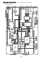
[1701] demodulates the video signal from the antenna input.
Tuner and IF-demodulator are in one unit. Also a modulator is
included in that part. The audio- and video-signal to the modu-
lator are the ones from the selected input or the playback path
of the set (“AMCO”- and “D_CVBS”-line). The control of the
tuner is fully done via I²C-bus by the CC-µP. Via the “MSW”-
signal and [7701] the modulator is switched on and off. In
opposite to this the antenna loop-through is opened or closed.
In the APAC-Pal version POS [1700] is used with the differ-
ence that it demodulates only PAL- instead of NTSC-signals
and has also no modulator. The “CSW_SSW” line switches the
modulator between CH3 or CH4 in the NTSC-version.
To achieve optimal tuning the “AFC”-signal is detected by the
CC via an analog input; [3701], [3702] and [3703] are used for
level adaptation (5V to 3V3). Pos [7700] is a driver for the
video signal.
The sound demodulation is realized by the MSP34x5 [7600],
which is also fully controlled via I²C-bus by the CC-µP (deter-
mination of bandwidth, amplitude, standard, …). The audio
signals are available at pin 30 and pin 31 of [7600] and fed as
“AFER”- & “AFEL”-line to the audio-I/O for further processing.
As this PCB is used for different regions (NAFTA and APAC)
either MSP3425 or MSP3415 are assembled.
Summary of Contents for DVDR880/001
Page 48: ...Mechanical Instructions EN 50 DVDR880 890 0X1 4 4 5 Dismantling Instructions Figure 4 14 ...
Page 166: ...Circuit IC Descriptions and List of Abbreviations EN 168 DVDR880 890 0X1 9 ...
Page 167: ...Circuit IC Descriptions and List of Abbreviations EN 169 DVDR880 890 0X1 9 ...
Page 174: ...Circuit IC Descriptions and List of Abbreviations EN 176 DVDR880 890 0X1 9 IC7411 ...
Page 182: ...Circuit IC Descriptions and List of Abbreviations EN 184 DVDR880 890 0X1 9 ...
Page 183: ...Circuit IC Descriptions and List of Abbreviations EN 185 DVDR880 890 0X1 9 ...
Page 184: ...Circuit IC Descriptions and List of Abbreviations EN 186 DVDR880 890 0X1 9 ...
Page 203: ...Circuit IC Descriptions and List of Abbreviations EN 205 DVDR880 890 0X1 9 ...

