Circuit-, IC Descriptions and List of Abbreviations
EN 165
DVDR880-890 /0X1
9.
9.6.3
Functional Description
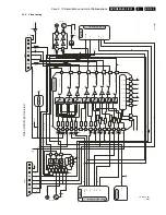
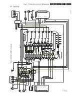
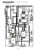
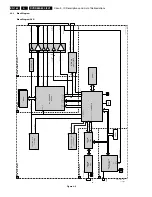
The DVIO module consists of the following blocks (see
blockdiagram):
1.
IEEE1394 Interface
•
PDI1394P25(7101)
•
PDI1394L40(7103)
2.
Micro-controller
•
89C51RD2(7203)
•
32kb SRAM(7201)
3.
FIFO and Control
•
FPGA/EPLD(7303)
•
SRAM(7301)
•
Clock generation(7307, 7308)
–
Independently tuneable audio and video clock,
implemented with FPGA and PLL
4.
DV-Decoder
•
NW700(7404)
•
EDO DRAM(7402, 7403)
5.
Audio & Video output
•
Audio DAC UDA1334ATS(7602)
•
Clock delay(7500)
•
Tristate buffer(7505)
IEEE1394 Interface
The 1394 interface consists of a PDI1394P25 physical layer
and a PDI1394L40 link layer.
It has the following features:
•
S200 operation (200 megabit per second)
•
One i.Link port (4 pin)
•
AV link port
Micro-Controller
The 89C51RD2 processor has a 8051 cpu with the following
extra features:
•
64 kilobyte of flash memory as program memory
•
1 kilobyte of internal data memory
•
watchdog timer
•
PCA outputs
•
Power control modes
•
Speed allowed up to 33 MHz but used at 11.0592 MHz
•
On board ISP(In Circuit Programming) functionality
ISP
By use of In Circuit Programming, it is possible to update the
software of the DVIO board that is in the 89C51RD2. ISP can
be made active by resetting the processor and keeping the
ISPN pin low during reset. During ISP, the ISPN signal on the
board has to be kept low. A programming voltage of 5V is
always present at the Vpp pin. When the ISP mode is active,
the new program can be sent to the microprocessor through
the serial port.
Fifo and Control
In decode mode, an isochronous AV-stream is flowing through
the IEEE1394 Interface into the FPGA. The FPGA stores the
data in a FIFO buffer (ping-pong buffer type, i.e. 2 buffers that
can hold one whole frame each).
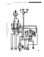
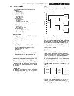
Reset
The FPGA controls the reset signals on the board. This has the
advantage that it is possible to reset the board both from
software and hardware.
Reset
Figure 9-5
The board reset NRESET will reset the whole board, and the
software reset can reset everything except the microprocessor
itself. Power-on reset is implemented by adding pull-ups and
pull-downs to the reset inputs of the devices. Since the FPGA
will tri-state all the pins during configuration, reset is active
during configuration time. After configuration of the FPGA, the
reset signals are driven inactive. The NRESET signal is used
to reset the DVIO board. After reset, the tri-state buffers to
connector 1500 are disabled.
Clock Circuit
There are 2 clocks to consider in the system, this is the video
clock and the audio clock. These two clocks do not have a
relation, so these clocks must be considered independently.
The video clock is approximately 27 MHz. When data is flowing
from an external source that is supposed to have the same
frequency, it does not have exactly the same clock. Because of
this, buffers may under-run of over-run. Since the clock can not
be directly recovered from the 1394 interface, there has to be
another solution. This solution is a tuneable clock that is
adjusted to the required frequency to process at the rate of the
incoming data.
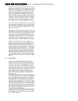
The hardware implementation of such a tuneable clock is as
follows:
Clock Circuit
Figure 9-6
The same can be applied for the audio clock. For this clock, a
frequency of 8.192 MHz, 11.2896 MHz or 12.228 MHz is
required. This depends on the sample-rate frequency(32kHZ,
44.1kHZ or 48kHZ)of the audio signal.
NRESET
DIGIT
AL BO
ARD
D
VIO BO
ARD
FPGA
PDI1394L21
SOFTWARE RESET
NW701
CL 16532095_120.eps
150801
ClockGen
(FPGA)
Raw clock
PLL
(CY2071)
slow-
loopfilter
regular clock
CL 16532095_121.eps
150801
Summary of Contents for DVDR880/001
Page 48: ...Mechanical Instructions EN 50 DVDR880 890 0X1 4 4 5 Dismantling Instructions Figure 4 14 ...
Page 166: ...Circuit IC Descriptions and List of Abbreviations EN 168 DVDR880 890 0X1 9 ...
Page 167: ...Circuit IC Descriptions and List of Abbreviations EN 169 DVDR880 890 0X1 9 ...
Page 174: ...Circuit IC Descriptions and List of Abbreviations EN 176 DVDR880 890 0X1 9 IC7411 ...
Page 182: ...Circuit IC Descriptions and List of Abbreviations EN 184 DVDR880 890 0X1 9 ...
Page 183: ...Circuit IC Descriptions and List of Abbreviations EN 185 DVDR880 890 0X1 9 ...
Page 184: ...Circuit IC Descriptions and List of Abbreviations EN 186 DVDR880 890 0X1 9 ...
Page 203: ...Circuit IC Descriptions and List of Abbreviations EN 205 DVDR880 890 0X1 9 ...

