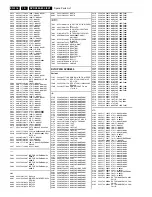
Circuit-, IC Descriptions and List of Abbreviations
EN 201
DVDR880-890 /0X1
9.
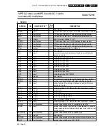
Pin Connections and Functions
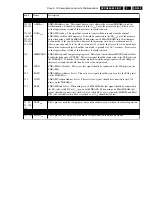
Pin #
Name
Description
See list
V
SS
Ground connections. Connect to the digital ground plane. Pins: 2, 17, 34, 55, 64, 74, 85,
96, 106, 115, 124, 132, 138, 145, 152, 159, 168
See list
V
DD33
Pad Ring digital power connections. Connect to the digital 3.3 volt power supply and
decouple to the digital ground plane. Pins: 1, 33, 63, 73, 84, 95, 105, 114, 123, 137, 144,
151, 167
See list
V
DD25
Core Logic digital power connections. Connect to the digital 2.5 volt power supply and
decouple to the digital ground plane. Pins: 16, 54, 107, 158
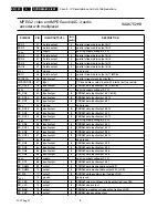
43
AV
SS
Ground connection for the clock PLL circuits. Connect to the digital ground plane
42
AV
DD
Analog power connections for the clock PLL circuit. Connect to a separately decoupled 2.5
volt power supply and decouple directly to the AV
SS
pin..
49
RESETB
Reset. When this input is set low it will reset all the internal registers to the default states.
Refer to the section on the control registers for details of these states. The device must be
reset after it is powered-up.
53
OE
When this pin is set high the outputs of the FLI2200 will be enabled; when it is set low the
outputs will be set into a high-impedance state.
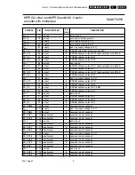
56-58
IFORMAT
2-0
Input signal format control. The settings of these pins set the format of the input signal.
This can be overridden by the IFmtOvr bit, bit 3 in register 00
H
, allowing this function to be
set or changed via the I
2
C bus. Please refer to the description of register 00
H
for details.
59-61
OFORMAT
2-0
Output signal format control. The settings of these pins set the format of the output signal.
This can be overridden by the OFmtOvr bit, bit 3 in register 07
H
, allowing this function to be
set or changed via the I
2
C bus. Please refer to the description of register 07
H
for details.
44-45
DADDR
1-0
The settings of DADDR
1-0
allow the device address of the control bus to be programmed to
prevent conflict with the other devices connected to the bus. DADDR
1-0
allow the device
address to be set to any of the following values: C0/C1
H
, C2/C3
H
, E0/E1
H
, E2/E3
H
. Please refer
to the section “Control Bus Operation and Protocol” for further information.
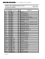
46
MODE
When this pin is set low the control bus will operate in the slave mode; allowing the device to
programmed from an external controller. When it is set high the FLI2200 will self-program from
an external I
2
C memory connected to the bus. Please refer to the “Control Bus Operation and
Control Protocol” section for more details.
47
SDA
2-wire serial control bus data. Data can be written to the control registers via this pin when it
is in the input mode and data can be read from the status registers when it is in the output
mode. Refer to the section on the serial port for timing and format details and to the section on
the registers for programming information.
48
SCL
2-wire serial control bus clock. When the control port operates in slave mode this pin will be
an input and when it operates in the self programming mode it will be an output.
40
PIXCLK
Pixel clock input. This clock is used to drive all the circuits in the FLI2200. An internal PLL is
used to upconvert this clock to provide the master clock signal and other clocks used
internally. Note that when the FLI2200 is used in the D1 input mode the PIXCLK input
should run at the rate of two cycles per pixel (one for luma and one for chroma).
62
N/P/IN/OUT
NTSC/PAL input or output. The default function of this pin is NTSC/PAL signal indicator
output. When the input video signal is a 525 line signal this pin will be set high and when it
is a 625 line signal the pin is set low. This function of this pin can be programmed to be an
input according to the setting of this pin if the NPOp
1-0
bits, bits 5-4 in register 03
H
, are set
to 00
H
, overriding the internal line counter. i.e., it will treat the signal as a 525 line signal
when it is set high and a 625 line signal when it is set low.
Summary of Contents for DVDR880/001
Page 48: ...Mechanical Instructions EN 50 DVDR880 890 0X1 4 4 5 Dismantling Instructions Figure 4 14 ...
Page 166: ...Circuit IC Descriptions and List of Abbreviations EN 168 DVDR880 890 0X1 9 ...
Page 167: ...Circuit IC Descriptions and List of Abbreviations EN 169 DVDR880 890 0X1 9 ...
Page 174: ...Circuit IC Descriptions and List of Abbreviations EN 176 DVDR880 890 0X1 9 IC7411 ...
Page 182: ...Circuit IC Descriptions and List of Abbreviations EN 184 DVDR880 890 0X1 9 ...
Page 183: ...Circuit IC Descriptions and List of Abbreviations EN 185 DVDR880 890 0X1 9 ...
Page 184: ...Circuit IC Descriptions and List of Abbreviations EN 186 DVDR880 890 0X1 9 ...
Page 203: ...Circuit IC Descriptions and List of Abbreviations EN 205 DVDR880 890 0X1 9 ...

