background image

5-2

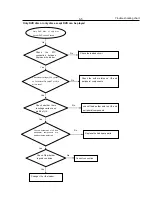
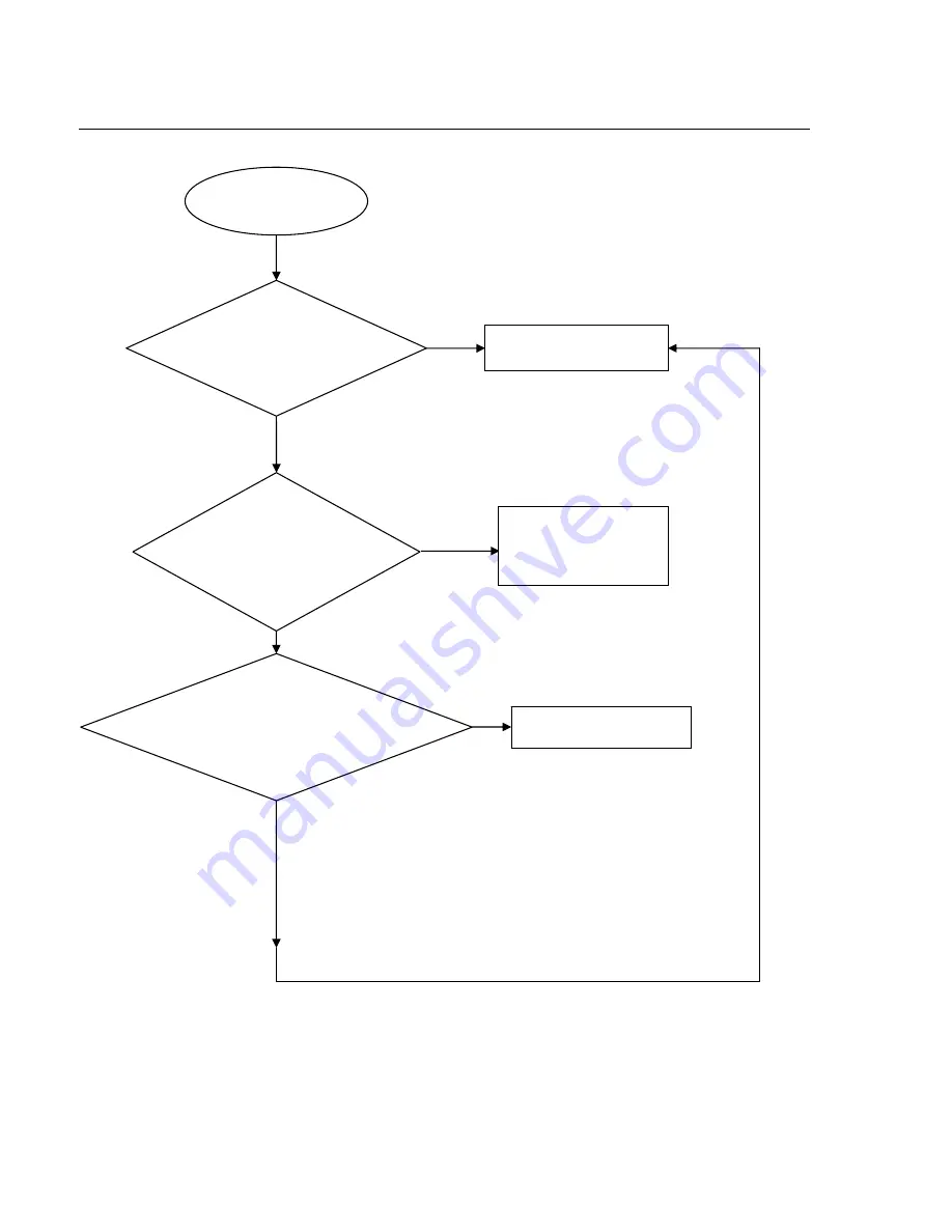
The power can not be on or off 

Go

Yes 

Yes 

No

No

The power can’t be 

on or off

Yes 

Repair the power board

Check the power supply 
on the power board is 
normal.

Check/Correct
connection  

Check if the xp1 on the 
decoderboard to XS301 on the 
frontboard is in good contact 

Correct the connection 

No

Yes 

Check if the CON2 on the 

power board to XP2 on the 

decoder board is in good 

contact. 

Trouble shooting chart 

Summary of Contents for DVP3320

Page 1: ...l Exploded view Part list 8 1 Copyright 2009 Philips Consumer Electronics B V Eindhoven The Netherlands All rights reserved No part of this publication may be reproduced stored in aretrieval system or transmitted in any form or by any means electronic mechanical photocopying or otherwise without the prior permission of Philips CLASS 1 LASER PRODUCT PHILIPS GB DFU Instruction 2 1 Revision List 9 1 ...

Page 2: ...cification Note 6SHFLÀFDWLRQ DQG GHVLJQ DUH VXEMHFW WR FKDQJH without notice Accessories supplied Remote control and batteries Audio video cables Power cable Playback media DVD Video Video CD SVCD Audio CD CD R CD RW DVD R RW DVD R RW Picture CD MP3 CD WMA CD 86 ÁDVK GULYH USB Compatibility USB Class support UMS USB Mass Storage Class TV standard Number of lines 625 PAL 50Hz 525 NTSC 60Hz Playback...

Page 3: ... wire between the two pins of the mains plug 2 Set the mains switch the on position keep the mains cord unplug 3 Measure the resistance value between the mains plug and the front panel controls and chassis bottom 4 Repair or correct unit when the resistance measurement is less than 1M 5 Verify this before you return the unit to the customer user ref UL standard no 1492 6 Switch the unit off and re...

Page 4: ...ch copper tracks and or components in this unshielded primary area when you service the player Service personnel must take precautions to prevent touching this area or components in this area A lighting stroke and a stripe marked printing on the printed wiring board indicate the primary side of the power supply Never replace modules or components while the unit is on 2 Laser The use of optical ins...

Page 5: ...ch off un used equipment or reduce heat x Mix of lead free solder alloy parts with leaded solder alloy parts is possible but PHILIPS recommends strongly to avoid mixed solder alloy types leaded and lead free If one cannot avoid clean carefully the solder joint from old solder alloy and re solder with new solder alloy SAC305 x Use only original spare parts listed in the Service Manuals Not listed s...

Page 6: ...r off in PBC mode d Navigation buttons Navigates through the menus Searches fast forward right or fast backward left Press repeatedly to change the search speed Searches slow forward up or slow backward down Press repeatedly to change the search speed e BACK Returns to the previous menu For DVD navigates to title menu For VCD version 2 0 or SVCD with PBC turned on returns to the menu f Previous Ne...

Page 7: ... channel on a disc n Stop Stops disc play o Play Pause Starts pauses or resumes disc play p INFO For discs displays information about the current status or the disc For slideshows displays a thumbnail YLHZ RI SKRWR ÀOHV q OK RQÀUPV DQ HQWU RU VHOHFWLRQ r SETUP Accesses or exits the setup menu 2 2 ...

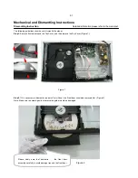
Page 8: ...the Top Cover Figure 1 Figure 1 Step2 If it is necessary to dismantle Loader or Front Panel the Front door should be removed first Figure 2 Note Make sure to operate gently otherwise the guider would be damaged Figure 2 3 1 Please kindly note that dismantle the front door assembly carefully to avoid damage tray and the front door Detailed information please refer to the model set ...

Page 9: ... Note Make sure to operate gently otherwise the guider would be damaged Figure 3 Step4 Dismantling Front Panel disconnect the connectors XP1 need release 4 snaps of Front Panel and 2 snaps of bottom cabinet then gently pull the Panel out from the set Figure 4 Figure 6 Figure 4 3 2 Detailed information please refer to the model set XP7 XP8 XP9 XP1 XP2 XP10 XP5 XP6 ...

Page 10: ...ing Instruction Figure 5 Step5 Dismantling Loader disconnect the 3 connectors XP7 XP8 XP9 aiming in the below figure and remove 1 screw that connects the loader and the bottom cabinet Figure 5 6 Figure 6 Detailed information please refer to the model set ...

Page 11: ... Instruction Step6 Dismantling Main Board first disconnect the connector XP2 and then remove 4 screws Figure 7 Figure 7 Step7 Remove the 4 screws on Power Board to dismantle the Power Board Figure 7 3 4 Detailed information please refer to the model set ...

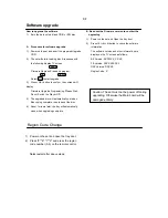
Page 12: ...omplete then take out the disc 5 About 1 minute later the tray will automatically close when upgrading complete B Read out the Firmware version to confirm the upgrading 1 Power on the set and Open the tray door 2 Press 9 6 6 button to check the software information The software version and other information are display on the TV screen as follows BE Version DVP33XX_XX XX FE Version XXXX XXXXXX DSP...

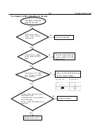
Page 13: ...nals 2 If there are F F T and T signals output from U4 Check Replace the loader Yes Yes No Go Check whether laser voltage 2 3V for DVD 1 9V for CD on Collector of Q4 and Q5 Check the FFC connection between 24P and the loader 1 Whether voltage on pin 97 of U2 varies between 0 and 3 3V 3 3V for CD and 0V for DVD 2 Whether peripheral components are eroded or badly soldered Trouble shooting chart Moto...

Page 14: ... board Check the power supply on the power board is normal Check Correct connection Check if the xp1 on the decoderboard to XS301 on the frontboard is in good contact Correct the connection No Yes Check if the CON2 on the power board to XP2 on the decoder board is in good contact Trouble shooting chart ...

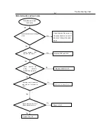
Page 15: ...Check whether U1 are eroded All output voltages on the power board is 0V or deviated Check whether there is 300V on C1 or C2 Check whether 100KHz oscillating signal on Pin6 of U1 Check if 5V 12V are short Check whether the components in the short circuit voltage are defected or eroded Yes Yes Yes Yes U1 PIN 3 RC waveform Trouble shooting chart Check whether F1 is blown ...

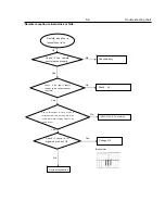
Page 16: ...connection between 24P and the loader Check U1 and peripheral components Re solder or replace the defective parts Check the connection between U2 Correct connection Replace U2 or loader Yes Check whether there is laser voltage 2 3V for DVD and 1 9V for CD on Collector of Q4 Q5 Check if there is RFO signal on pin10 of XP7 The normal RFO signal is a clear reticulated wave Trouble shooting chart Chec...

Page 17: ... components Check whether there is voltage variance on pin 88 of U2 check if bad solder exist on U2 and peripheral components Replace the bad spare parts Check whether pins of U2 and peripheral components are badly soldered defected Check Q4 whether in good condition Yes Yes Yes Go Correct connection Change U2 or the loader No No Yes Check laser voltage 2 3V output on Collector of Q4 if pin87 of U...

Page 18: ...it Check the U2 s pin 48 95 96 arrive the XP1 connect condition Correct connection Replace U301 or LED Yes Yes Yes No Check VCC 5v voltage on the power and front board Check there are CS DATA and CLK signals on XS301 on the front board 1 Check whether bad solder exists on U600 and pins of LED 2 Check whether the circuit connected to K301 K302 is broken 3 Check whether R303 R301 R302 are open circu...

Page 19: ...ormal change the power board Replace Q8 Q10 Q12 Check whether R73 and R77 are normal Yes Check whether the muting transistor Q8 Q10 Q12 are normal Checking the U5 leads the feet has no to break to open RUUHFW FRQQHFWLRQ Check whether the U7 or U8 powersupply normal No Yes Check the power supply voltages 12VA Yes Check U7 U8 Replace U7 or U8 No Trouble shooting chart ...

Page 20: ... decoder board are normal Check Y2 R28 C31 and C33 Check other of power supply electric circuit Correct the connection Check whether the video filter network circuit is normal Yes Yes No No No Check whether the 27MHz output signal Trouble shooting chart change U2 Yes No Check if the video signals on Pin 58 60 61 63 of U1 are normal ...

Page 21: ...n oscilloscope to check if there is output waveform from the first pin IR of the remote censor after pressing button on the remote control IR600 PIN1 RC waveform Check if there is IR signal on pin 49 of U2 Check if the power supply voltage to the remote censor is normal Go No No No Yes Yes Yes Correct connection Yes Change U2 IR waveform Trouble shooting chart ...

Page 22: ...rcuit Crystal oscillator Y2 and peripheral components are defected or eroded No No No Yes Yes Yes 27Mhz waveform Trouble shooting chart Check whether all the voltages from the power board to the decoder board are normal CVBS R1 point waveform Check if there is 135MHz signal output on R31 Check whether short circuit or bad solder on U1 U3 SDRAM R31 PCLK waveform Check U2 No No Reconnect the compone...

Page 23: ...B WIRING DIAGRAM 1 6 DVD LOADER 5PIN 2 0 6PIN 2 0 5PIN 2 5 24PIN 0 5 5PIN 2 5 CVBS 6 Pb Pr XP2 CON2 6PIN 2 0 XS301 3 8PIN XP1 XP9 XP8 XP7 P1 P2 XS302 4PIN 2 0 1 5 6 ZR36966XE2 XF2 AM5888S 8M 16M FLASH 64M 16M SDRAM AUDIO AMP LPF MOTER DRIVER XP1 SWITCH BOARD 4PIN 2 0 4 1 ASA SANYO DV38 Y 6PIN 2 0 VIDEO LPF DRIVE 1 4 1 L COAX 1 R 1 1 4PIN 2 0 XP11 4 XP601 4 7PIN USB 4PIN 2 0 4 1 DOWN LOAD XP5 6 1 6...

Page 24: ...G5 KS5 12 SEG6 KS6 13 SEG7 KS7 14 GND 28 GRID1 27 GRID2 26 GND 25 GRID3 24 GRID4 23 GND 22 VDD 21 SEG14 GRID5 20 SEG13 GRID6 19 SEG12 GRID7 18 SEG10 KS10 17 SEG9 KS9 16 SEG8 KS8 15 CE300 47uF C310 0 1uF R320 0R C315 47p C309 0 1uF R318 100R NC CE301 47uF R307 10K R308 10K R303 4K7 R309 1K R304 4K7 K301 open close R305 4K7 REM301 REM IR 1 GND 2 VCC 3 4 4 5 5 C304 100p C305 100p C316 100p R310 1K R3...

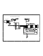
Page 25: ...A A B B C C D D E E 1 1 2 2 3 3 4 4 SWITCH BOARD C319 47p C317 47p C318 47p XP1 CON4 2 0 1 2 3 4 LED3 K303 POWER Switch Board Electric Diagram for DVP3320 7 2 7 2 ...

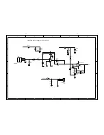
Page 26: ...08 100p R202 22K C203 1000p R206 20K U5A NJM4558 OPA 3 2 1 8 4 R209 750R CE200 22uF C210 2 2uF C206 47p R205 180K R211 100K R210 150 R203 22K R208 1K R200 10K CE202 10uF C201 0 1u C205 47p CE201 22uF R201 20K C211 2 2uF NC R207 100K 3PIN 2 0mm XP601 1 2 3 C204 100p U5B NJM4558 OPA 5 6 7 8 4 C209 2 2uF OK Board Electric Diagram for DVP3320 7 3 7 3 ...

Page 27: ...INPUT 1 2 C2 15uF 400V 250V 450V D1 1N4007 R7 1 6W11 3k 1 D5 FR102 R13 1 6W100k T1 EEL19 8 6 3 5 9 12 10 4 7 11 1 P3 1 D3 1N4007 C5 152 1KV R9 1 6W10k CON1 AC INPUT 1 2 L2 6 8uH U3 TL431 2 1 3 F1 T2AL 250ac D2 1N4007 C1 10uF 400V 250V 450V TR1 NTC 10 20 R1 NU R5 1 6W12K 1 CON2 6X2 5 HEADER 5V 1 5V 2 GND 3 12V 4 GND 5 22V 6 R8 1 6W1k P2 1 C7 1000uF 16V D4 1N4007 R2 1 4W120K U2 PC123X92 1 2 4 3 C3 1...

Page 28: ...ing 20mA L3 0R C18 47pF C17 0 1uF R13 4 7K R90 100R C88 0 1uF C15 150pF D10 PESD5V0S L 1BA 2 1 C4 150pF C12 150pF C3 150pF R9 NM Q2 BT3904 R3 33R D12 PESD5V0S L 1BA 2 1 D11 PESD5V0S L 1BA 2 1 6PIN 2 0mm XP1 1 2 3 4 5 6 D9 PESD5V0S L 1BA 2 1 C16 0 1uF L4 0R Q3 8550D C14 150pF R7 4 7K C2 100pF 5PIN 2 5mm XP2 1 2 3 4 5 R86 100R U11 PESD3V3L5UY 1 2 3 4 5 6 R6 4 7K 47 RCA151 XX1 RCA P1 RCA AUDIO OUT 1 ...

Page 29: ... C91 0 1U CE2 100U 16V U10 NM 64Mbit K4S641632H UC70 VDD 1 DQ0 2 VDDQ 3 DQ1 4 DQ2 5 VSSQ 6 DQ3 7 DQ4 8 VDDQ 9 DQ5 10 DQ6 11 VSSQ 12 DQ7 13 VDD 14 DQML 15 WE 16 CAS 17 RAS 18 CS 19 BA0 20 BA1 21 A10 22 A0 23 A1 24 A2 25 A3 26 VDD 27 VSS 28 A4 29 A5 30 A6 31 A7 32 A8 33 A9 34 A11 35 NC 36 CKE 37 CLK 38 DQMH 39 NC 40 VSS 41 DQ8 42 VDDQ 43 DQ9 44 DQ10 45 VSSQ 46 DQ11 47 DQ12 48 VDDQ 49 DQ13 50 DQ14 51...

Page 30: ...OPU HD65PS Others R34 3 3R 4 7R R38 3 3R 4 7R Close to Vaddis Imax 600mA Õ 540mA ǂ Imax 300mA Õ I 290mA ǂ Imax 300mA Õ 250mA ǂ OPU R270 R283 HOP1200W 100R 100R Arima681 100R 100R Others NM NM R47 51K 27K R40 100R NM C61 27nF C57 0 1uF R46 1K 6PIN 2 0mm XP8 1 2 3 4 5 6 L11 10uH R51 2 2 OHM 2W R43 0R 300R CE6 220uF 16V R34 4 7R 5PIN 2 0mm XP9 1 2 3 4 5 CE5 220uF 16V C65 NM 1nF C55 100pF R48 51K 27K ...

Page 31: ...9012 C74 1uF NC R73 4 7K C72 1 2nF C80 100pF U5A LM4558 3 2 1 8 4 R80 100R R76 470 C70 0 1uF CE13 10uF 16V R61 82K R96 1k R63 4 7K C68 75pF C78 0 1uF R72 4 7K R79 100K C81 100pF R62 39K C77 100p R103 4 7K NC CE18 47uF 16V R74 470 C69 1 2nF R70 82K C71 75pF R71 39K XP10 pitch 2 0mm 3 1 2 3 D7 BAT54S NC 1 2 3 Q11 3904 R83 100 Q10 9012 R67 470 R82 33K R77 4 7K R64 4 7K C75 3300p CE14 220U 16V R78 22K...

Page 32: ...Front Board Switch Board Print layout Bottom side 7 9 7 9 ...

Page 33: ...OK Board Print layout Top side OK Board Print layout Bottom side 7 10 7 10 ...

Page 34: ...Power Board Print layout Bottom side 7 11 7 11 ...

Page 35: ...Main Board Print layout Top side 7 12 7 12 ...

Page 36: ...Main Board Print layout Bottom side 7 13 7 13 ...

Page 37: ...ed View for DVP3320 55 It s a general mechanical view for DVP3320 55 pls refer to the model set for detailed information Assy 1 component includes 1 3 4 5 21 1 2 3 4 5 6 7 8 9 10 11 12 13 14 15 16 17 18 19 20 21 ...

Page 38: ... 12NC No Description Q ty Q12 996510009669 SMD TRANSISTOR MMBT3904LT1 NPN 1 7 S T SCREW B 2 6 X 8 BF 6 Q13 996510009669 SMD TRANSISTOR MMBT3904LT1 NPN 1 12 S T SCREW B3 X 6 BF 9 Q14 996510009669 SMD TRANSISTOR MMBT3904LT1 NPN 1 14 S T SCREW B 3 X 7 BF 5 Q2 996510009669 SMD TRANSISTOR MMBT3904LT1 NPN 1 Q3 996510009671 PNP TRANSISTOR 1 Q4 996510021453 SMD TRANSISTOR MMBT8550CLT1 1 Q5 996510021453 SM...

Page 39: ...REVISION LIST Version 1 0 Initial release for DVP3320 55 9 1 ...

Reviews: