Circuit descriptions and abbreviation list
GB 90
EM1A
9.
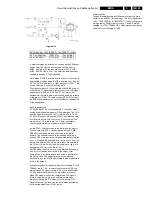
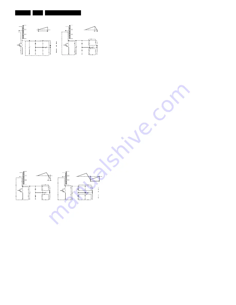
Figure 9-9
Period t1 - t2:
When TS7421 is driven into conductivity, the capacitor
voltage of 141 V, will be divided across bridgecoil L5422 and
the deflection coil (conn. 0317). Due to the chosen
inductance values, there will be 100 V across the deflection
coil and 41 V across L5422. The linear increasing current in
the deflection coil will result in a spot moving from the centre
of the picture tube to the right.
The voltage across L5422 will also charge C2421 (41 V - 0.7
V).
Period t2 - t3:
At the moment the LINEDRIVE signal becomes high,
TS7421 will stop conducting. In the coils a voltage will be
induced, trying to maintain the current. The current through
the line deflection coils continues to flow through C2425 and
C2421 and the current through L5422 continues to flow
through C2426 and C2421. The energy stored in the line
deflection coil is passed to C2425, and the energy of L5422
to C2426.
The resonance-frequencies of these 2 LC-circuits define the
flyback time of the spot from the right side of the picture tube
to the left.
On average no current flows through C2421 and thus the
voltage across this capacitor remains constant.
Figure 9-10
Period t3 - t4:
As for the period t2 - t3; but now the current flows in the
opposite direction, since the voltage across C2425 and
C2426 is higher than the voltage across C2433 and C2421.
Period t4 - t5:
The coils want to maintain the negative current and will
charge the capacitors negative. Because of this, D6422 and
D6423 will conduct. The voltage is 100 V across the
deflection coil and 41 V across L5422. As both diodes
conduct, we may consider the voltage to be constant. A linear
current flows with the same changing characteristics as in
period t1 - t2. The spot now moves from the extreme left of
the picture tube to the centre. Before the current becomes
zero, and the spot is located in the centre of the frame,
TS7421 reverts back into conductivity. First a short negative
current will flow. The cycle starts again.
The linearity correction
A constant voltage across the horizontal deflection coil
should result in a linear increasing saw-tooth current. This
however is not the case as the resistance of the coil is not
negligible. In order to compensate for this, a pre-magnetised
coil L5421 in series with the deflection coil is used. This coil
ensures that during time interval t1 - t3 the circuit-resistance
will be higher than during t4 - t5. L5421 is called the linearity
coil.
To avoid self-oscillation, R3431 and C2431 are placed
parallel to L5421.
The S-correction
Since the sides of the picture are further away from the point
of deflection than the centre, a linear saw-tooth current would
result in a non-linear image (the centre would be scanned
slower than the sides). To solve this, the deflection current for
the right- and left side will be reduced.
C2433 is charged quadratic during time interval t1 - t2. Left
and right the voltage across the deflection coil decreases,
causing the deflection to slow down. In the centre, the
voltage increases and the deflection will be faster. An S-
shaped current will have to be superimposed onto the saw-
tooth current. This correction is called finger-length
correction or S-correction. C2433 is relatively small, as a
result of which the saw-tooth current will generate a parabolic
voltage with negative voltage peaks. The current also results
in a parabolic voltage across C2421, resulting in the finger-
length correction, proportionally increasing with the picture
width. The EW-DRIVE signal will ensure the largest picture
width in the centre of the frame. Here the largest correction is
applied. The larger the picture width, the higher the deflection
current through C2433.
The E/W-correction
A line, written at the upper- or lower side of the screen, will
be larger at the screen centre when a fixed deflection current
is used. Therefore the amplitude of the deflection current
must be increased when the spot approaches the screen
centre. This is called East/West correction.
The EW-DRIVE signal is generated in the HOP and will drive
FET TS7480 via TS7481 and optocoupler TS7482. TS7480
will charge capacitor C2423 more or less, increasing the
deflection current when reaching the centre of the screen.
Secondary line-voltages
During the blocking time of TS7421, the magnetic energy of
coil 1 - 5 of the LOT will be transferred to electrical energy in
the secondary winding. Via rectifying and smoothing, the
several secondary supply voltages will be generated:
•
EHT, Focus and Vg2-voltage
•
+180V for the CRT panel (pin 8 LOT)
•
+11D for the line deflection (pin 12 LOT)
•
+13VLOT for the frame deflection (pin 6 LOT)
•
-15VLOT for the frame deflection (pin 3 LOT)
•
Filament voltage (pin 9 LOT)
•
The EHT-INFO signal is derived via R3450//R3451. This
signal decreases while the beam current increases. It is fed
to the HOP to compensate for loss of picture width and
picture height.
The DYN-FASE-CORR signal is fed to the HOP via C2455
and drives a dynamic phase correction necessary because of
beam current variations. This is done by regulating TON of
the line transistor TS7421.
East-West circuit
The moment TS7480 is driven into saturation, C2421 will
discharge during the flyback. As a consequence of which
C2421 must be charged again during the scan via the
conduction diode D6422 (as long as C2421 is not charged to
the voltage across L5422, D6422 will conduct). The current
in the deflection coil is therefore larger than the current
CL 96532156_024.eps
060199
141V
7421
Line defl.
2433
5422
6423
6422
2425
2426
2421
Defl
t2
t3
5430
141V
7421
Line defl.
2433
5422
6423
6422
100V
141V
41V
2425
2426
2421
I
Defl
t2
t1
41V
5430
+
-
I
2420
2420
CL 96532156_025.eps
231299
141V
Line defl.
2433
5422
2425
2426
I Defl
t3 t4
5430
141V
Line defl.
2433
5422
6422
2425
2426
I Defl
t5
t4
5430
100V
141V
41V
+
-
7421
7421
2420
6423
6422
6423
2420
2421
41V
2421
41V

