Circuit Descriptions, Abbreviation List, and IC Data Sheets
9.
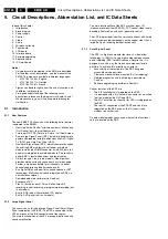
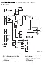
The HIP1 delivers YUV and sync signals to the PICNIC (in the
Feature Box). This IC takes care of:
•
Analogue to Digital conversion and vice versa.
•
100 Hz processing
•
Interlaced to progressive scan conversion.
•
Panorama mode.
•
Noise reduction.
•
Dynamic contrast.
After the PICNIC, the YUV-signals are fed to the FALCONIC for
"Natural Motion", followed by the Eagle for "Pixel Plus"
enhancement (if present). The processed YUV signals (from
Eagle or PICNIC) are, together with the sync-signals from the
PICNIC, then fed to the HOP (High-end Output Processor).
This IC handles the video control and geometry part. The RGB-
signals for CC/OSD (from the uP) are also inserted via the
HOP. The video part delivers the RGB signals to the CRT-
panel and the geometry part delivers the H-drive, V-drive, E/W-
drive, and TILT-drive signals.
Both deflection circuits are "hot" and located on the LSP. The
HOP drives them. To make a galvanic separation, the Line
Drive is driven via transformer 5410 and the Frame Drive via
transformer 5621.The horizontal output stage generates some
supply voltages and the EHT voltage, focus voltage and Vg2
voltage.
The RGB amplifiers on the CRT-panel are supplied with 200 V
from the LOT.
The Auto-SCAVEM circuit modulates transitions of the
Luminance (Y) signal on the horizontal deflection current,
giving a sharper picture.
The sound part is built around the MSP44x2 (Multi-channel
Sound Processor) for IF sound detection, sound control and
source selection. Dolby decoding is done by two separate ICs
in cooperation with the MSP. Amplification is done via a "class
D" integrated power amplifier IC, the TDA7490.
The set is also provided with a "wireless out" connector, for
wireless surround applications.
The microprocessor, called OTC (OSD, TXT/CC and Control)
takes care of the analogue TXT input processing and output
processing. The OTC, ROM, and RAM are supplied with 3.3 V,
which is derived from the +5V2.
The NVM (Non Volatile Memory) is used to store the settings;
the Flash-RAM contains the set software.
There is a separate Standby Supply, in order to reduce the
Standby power consumption. During Standby, the Main Supply
is switched "off" (via TS7529).
A relay (1550) is used to switch the Degaussing circuit. It is
switched "on" after set start-up and switched "off" by the
microprocessor after 12 s.
The Main Supply, a SMPS based on the "boost converter"
principle, generates the 141 V (V_BAT) and the +/- 16 V for the
audio part.
For the power supply of the FBX and DW/PIP circuits, a
separate DC/DC converter is used, generating 3.3 V.
9.3
Power Supply
The power supply has a number of main functions:
•
Mains harmonic filter. The mains harmonic filter has two
functions: to prevent high frequency signals (harmonics)
from being transferred into the mains and to protect the set
from lightning damage.
•
Degaussing picture tube. As soon as the set is switched
"on" via the ON/OFF switch, the 5V2 is present. When the
DEGAUSSING signal from the processor (OTC) is "low",
transistor 7528 will conduct, and relay 1550 is activated.
Initially a considerable current will flow, via PTC 3516,
through the degaussing coil. The PTC will heat up,
resistance will rise, and the current will decay rapidly. The
OTC makes the DEGAUSSING signal "high" after 12 s,
which will switch "off" the relay.
•
Standby supply:
–
Fly-back supply principle.
–
Outputs: 5V2, 8V6, 12V, and 30V.
•
Main supply:
–
Buck-boost supply.
–
140V (not mains isolated).
–
+16V and -16V for audio.
–
Self-oscillating power supply (SOPS).
•
DC/DC converter. The function of this part is 12 V to 3.3 V
conversion, to provide the supply voltage for the Feature
Box and DW/PIP Muppet.
9.3.1
Standby power supply (diagram A2)
Compared to the EM5 circuit, there are the following
differences in the +5V and +8V Standby power supply.
•
The +5V is protected against over-voltage via D6149 and
TS7140.
•
If the +11V (11V_STBY line) is not present, the +5V supply
line will be switched "off" via TS7141.
9.3.2
Main Supply (diagram A1)
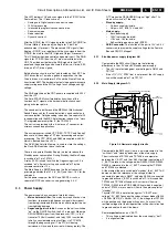
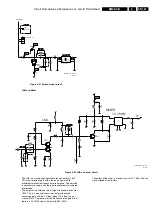
Figure 9-4 New main supply circuits
Compared to the EM5 circuit, there is an improvement in the
"switch off" and "standby" behaviour of the main supply.
The circuit around TS7505 and TS7508 is a comparator
between the V_BATT and the +380 V rectified input voltage. If
V_BATT is present, the voltage divider R3554, R3555, R3560,
R3556 is referenced to the +V_BATT, meaning that TS7505
and TS7508 are blocked.
At the moment the set is switched to "standby", the V_BATT will
decrease. Now the reference of the voltage divider is
connected to ground via R3557, and also R3556 is connected
to ground because V_BATT is switched "off". In this condition,
TS7505 and TS7508 will conduct. A current will flow via
TS7508 / R3559 to the SUP-ENABLE line (which is negative),
and via TS7529 more current will flow in the opto-coupler for
"standby".
Thyristor TS7503 is a protection against "V_BATT over-
voltage". If V_BATT exceeds the values of zener diodes D6524
+ D6508 + D6513 (47+56+56= 159 V), then the gate of TS7503
will be positive and the device will conduct. As a result, the
rectified voltage after the bridge rectifier will be short-circuited
to ground and the fuse will be blown.
Some important notes on V_BATT:
•
This voltage is not isolated from the main supply ("hot").
•
It is alignment free.
CL 36532008_130.eps
080503
COLD
RES
HOT
HOT
TO
COLD
RES
FOR LATAM - AP SETS
0301 OF
3551
330R
3548
1K
1M2
3560
BZX384-C56
6513
F528
I576
10K
3559
3561
1M
10u
2539
6M
8
3554
3502
4M7
6508
BZX384-C56
2n2
2505
GND-SSP
BZX384-C47
6524
BF423
7508
3558
47K
1510
2545
1n
2529
100n
7503
BT151
9512
9514
BC857B
7505
MCL4148
6522
220K
3557
3556
47K
680K
3555
4M7
3503
2521
470p
GND-SUP
VBATT
VBATT
TUNERGND
Improved switch off and Standby
Vbatt
OVP Protection


