Circuit Descriptions, Abbreviation List, and IC Data Sheets
9.
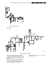
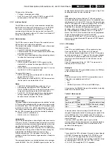
+3V3 Detection
If the +3.3V and +5V are present, C2U26 is charged. Transistor
T7U10 conducts, T7U11 is blocked, and the PWM and Driver
circuit is working.
If there is a voltage drop on the +3.3V, the voltage on C2U25
cannot be maintained, resulting that T7U10 will block and the
PWM and driver circuit will be switched "off".
+5V Detection
The same situations if the +5V drops: T7U07 and T7U13 will
block, the reference voltage on R3U41 will drop, and a switch
"off" of the PWM and Driver circuit is the result.
Diode 6U06 is foreseen to clamp the output voltage to 5 V in
case of fault conditions (like 7U04 short-circuited D-S). The
fuse 1U01 will open in such conditions.
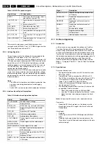
Role of Other Components
•
The capacitors 2U06 and 2U10 are filtering the ripple
current generated by the commutation of power MOS-FET
7U04 (about 700 mA_rms, while the capacitor 2U08 is
filtering the output voltage.
•
Coil 5U02 and capacitor 2U15 prevent that noise
generated by the switching will disturb other circuits
supplied from +11V.
•
Coils 5U05 and 5U06 and capacitors 2U23 and 2U31 are
supplementary filtering of the output voltage for the two
load circuits (PIP and Feature Box).
•
Beads 5U03 and 5U04 damp oscillations during the
switching of the power MOS-FETs.
•
Components 2U01, 2U02, and 6U02 are not present (the
voltage “+3V3-ILINK” is not used).
Service Tips
•
When a power MOS-FET is found defective, replace the
other power MOS-FET, the fuse 1U01, and the diode 6U06
as well.
•
When a driver transistor (7U01, 7U02, 7U08, or 7U09) is
found defective, replace the complementary transistor as
well
(example: replace also 7U08 if 7U02 is defective).
•
For a normal operation of the converter, it is important to
check the switching frequency, the value of the boost
voltage, and the amplitude of the gate voltage of transistor
7U04 (it should be close to the boost voltage).
9.4
Control
9.4.1
"Switch On" Behaviour
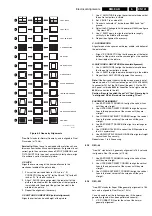
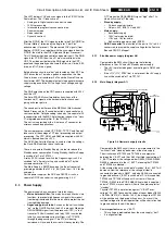
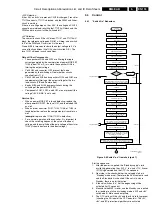
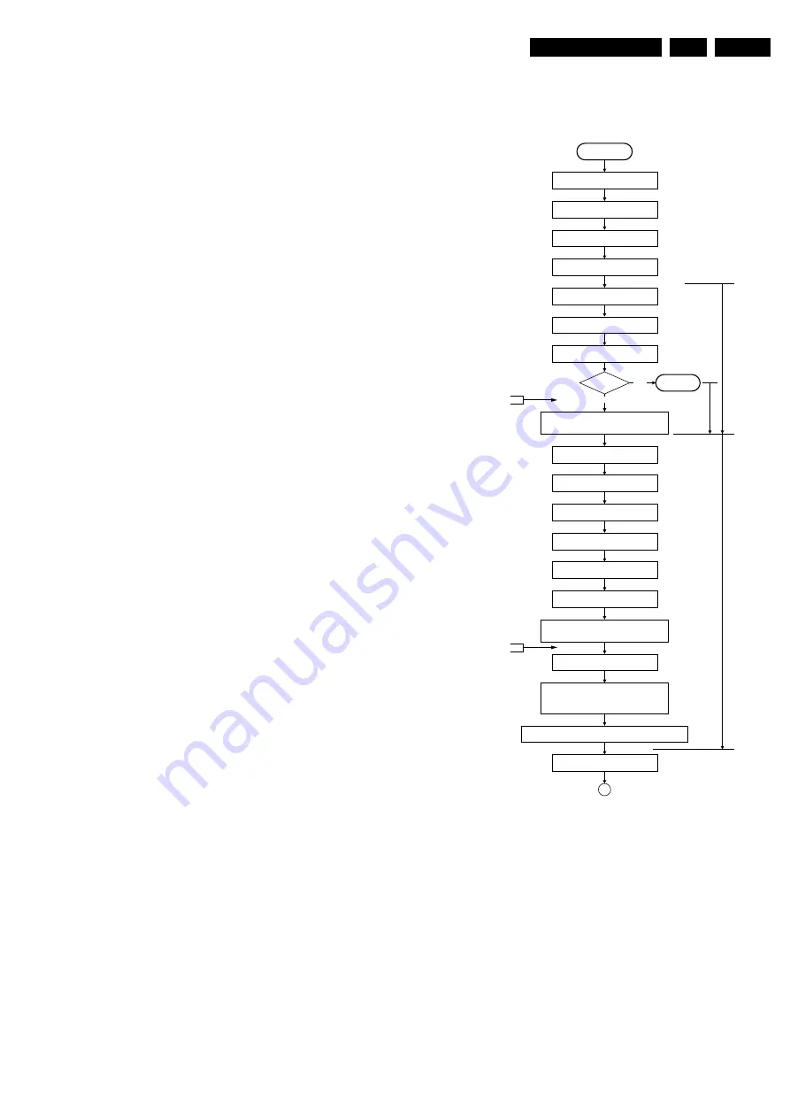
Figure 9-6 Switch "on" flow chart (part 1)
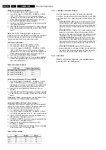
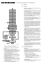
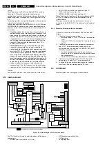
Start up sequence:
1.
After the power is applied, the "Standby supply" starts
oscillating, generating the +5V2, V_tun, and +11V. A reset
(POR) is generated and the OTC is awakened.
2.
Next step is the check whether the set needs to be in
"Standby" mode or not. Therefore, the NVM content is read
and the Standby-bit is checked. If the set is to stay in
Standby, there is no further action.
3.
If the set switches "on", first the degaussing will be
activated (for 12 seconds).
4.
Meanwhile the MSP is reset, and the Standby line is pulled
low, leading to a full semi standby mode (+5V2 and +8V
switched on). Mute sound amplifiers.
5.
The OTC waits until the +5V and the +8V are fully present
(checking the AD-input of the OTC does this). The +5V,
+8V, and I2C protection-algorithms are activated.
CL 36532008_124.eps
080503
off state:
Power is applied
Standby supply starts running.
+5.2V; Vtun; +11V become present
OTC resets
Initialise I/O pins of the OTC
Initialise HDD interface
Initialise DVD interface
Read IO exp DVD
Read NVM identification and
standby bit; enable watchdog
Standby bit
set?
Activate degaussing and
deactivate after 12 seconds (of course, in the
meanwhile, other processes should continue)
start HDD
activate MSP reset
Put Standby line LOW
Keep sound amplifiers
muted with sound enable = HIGH
+5V and +8V is switched ON
+8V and +5V get their nominal
level, detected by the OTC
activate protection algorithms for +8V
and +5V and I
2
C (start I
2
C protection the
moment the component is initialised)
Read rest of NVM information
Initialise HOP; set_sync_mode = not_active
set_black_current_stabilisation = not active
set_standby_mode_HOP = ON
set_rgb_blanking = ON
Initialise HIP: IF, source selection, 2fh input, video processing
Switch on the syncoutput: set_syncout_tristate = OFF
Initialise 3D Combflter
Only in US sets (not in 2003)
Set stays in
standby mode
No
Yes
t<1500ms
t<500ms
t<250ms
Trapped Startup 2
Trapped Startup 1
A


