Circuit Descriptions, Abbreviation List, and IC Data Sheets
9.
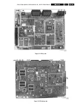
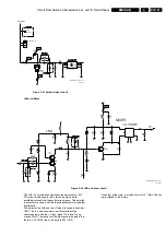
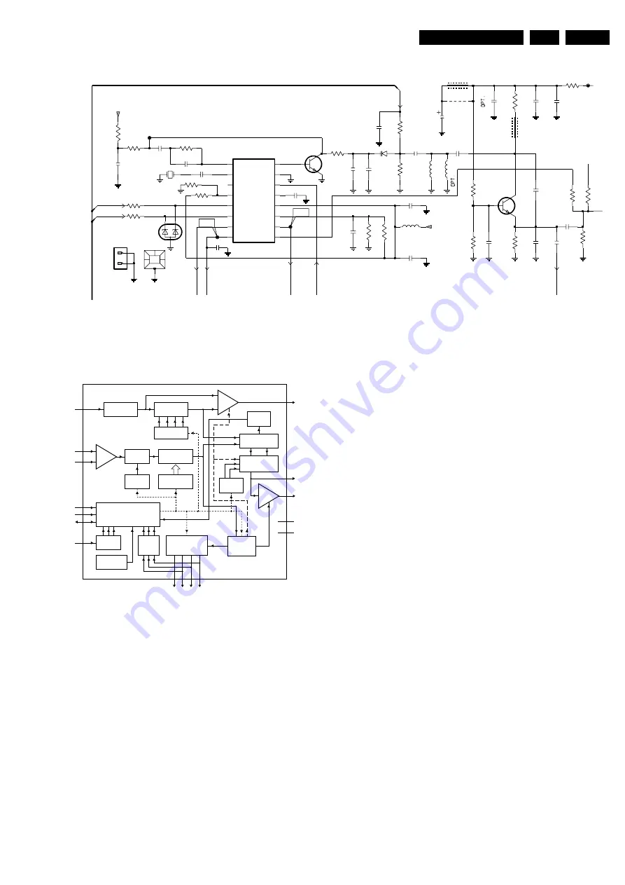
Synthesizer and Local Oscillator
Figure 9-17 Synthesizer and local oscillator
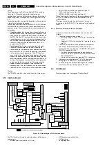
The internal circuitry of the synthesizer IC (TSA5060A) can be
seen in figure below:
Figure 9-18 Block diagram TSA5060A
The TSA5060A is software controlled by the I2C bus
(commands are send directly via the TV slow I2C bus).
To verify whether there is communication between the host
device and the TSA5060A, one can check the supply voltage
of the oscillator transistor 7103 (TP F113). This should be
about 7.5 V in normal conditions when the I2C signal is
interpreted by the synthesiser. If there is improper
communication, the voltage remains at 0 V.
There is version recognition foreseen to discriminate between
433 or 864 MHz units. This feature will automatically load the
correct frequency division words into the synthesiser at starting
up and initialisation of the TV set.
The reference quartz crystal is 4 MHz, which is divided to a
lower reference frequency of 25 or 50 kHz (depending on the
version).
The PLL filter is passive and includes 2103, 2104, and 3107.
The transistor 7102 is part of the PLL current source, and
allows connection to higher supply voltages as +5 V.
The TSA5060A has some output ports:
•
Port P3 (V_osc), used to switch the local oscillator (LO).
•
Port P2 (V_pil), used to switch the pilot.
•
Port P1, used to switch the power amplifier (PA).
The local oscillator (LO) is a common base transistor (7103)
that is oscillating at half the output frequency. The frequency is
tuned by varicap 6102, until the tuning voltage is in the range
of the loop filter (between 1 and 6 Vdc). If the voltage is outside
this range, then possibly the division ratio is chosen outside the
normal range, or some frequency dependant component
around the transistor is faulty.
SYNTHESIZER
3114
15K
2198
220p
3107
2K2
4107
1K0
3103
PLVA2656A
6101
5132
BLM21
3113
6K8
5p6
2111
3112
100K
12n
5113
470R
3101
2201
100p
2107
1n0
3102
470R
2108
22p
10K
3111
BC847B
7102
1107
Hole 3.5 mm
1
2
100n
2114
5103
BLM21
3106
100R
6K8
3105
2115
220p
2118
1p
F113
3110
AT-51
1105
4M
330R
0001
frame
1
2
3
4
5
2116
15p
2113
6p8
7103
BFR92A
10u
2103
10n
2101
1n0
2106
2199
10u
220p
2122
100n
2104
4K7
3109
2K2
3108
3121
82R
P2
7
P3
13
RFA
14
RFB
6
SCL
5
SDA
12
VCC
2
XTAL
3
XT|COMP
330R
3119
TSA5060ATS
7101
11
ADC
4
AS
1
CP
16
DRIVE
15
GND
10
P0
9
P1
8
F112
F111
3115
150R
5101
100n
5108
12n5
470p
2109
1K0
F110
3104
18p
2102
15p
2117
6K8
3120
6102
BB151
470n
2110
220p
2197
3122
2K2
2120
1p8
3116
100R
220n
2105
I2C_data
I2C_clock
MPX
Vpil
Vosc
OSC
OSC
mon_ster
+8b
+5V
CL36532008_070.eps
290403
CL36532008_071.eps
010503
FCE717
PRE
AMP
AMP
LOCK
DETECT
DIGITAL PHASE
COMPARATOR
CHARGE PUMP
REFERENCE
DIVIDER
DIVIDER
1/2
17-BIT
DIVIDER
17-BIT LATCH
DIVIDE RATIO
I
2
C-BUS
TRANSCEIVER
1-BIT
LATCH
2-BIT
LATCH
3-BIT
ADC
POWER-ON
RESET
MODE
CONTROL
LOGIC
3-BIT
INPUT
PORTS
4-BIT LATCH
AND
OUTPUT PORTS
XTAL
OSCILLATOR
4-BIT LATCH
2
XTAL
13
RFA
14
RFB
4
AS
6
SCL
5
SDA
11
10
9
8
7
ADC
CP
1
XT/COMP
3
DRIVE
16
VCC
12
GND
15
TSA5060A
P3 P2 P1 P0


