Circuit Descriptions, List of Abbreviations, and IC Data Sheets
EN 89
F21RE AB
9.
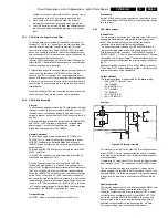
settled. This means a wait state of 100 ms, after the crystal
configuration of the HIP has correctly been read out.
3.
Next, all other ICs are initialised. Now, the E-box is
working, but the monitor is still not displaying a picture.
4.
The HOP switches on the PHI1 loop, the software sets all
the necessary video and audio parameters, and enables
them.
9.2.3
PSU: Mains Voltage Inlet and Filter
The Mains voltage is provided by inlet 0300, after which it is
fused by a T2.5A fuse. The next part, the Mains voltage filter,
consists of an LC-common mode filter section. This filter
consists of two capacitors (items 2002 and 2004) from both
phase and neutral to ground (to reduce the leakage current)
and an inductor (5000). Interferences on one of the phases are
shorted to ground by these capacitors.
Inductor 5000 also provides a differential-mode filtering with
capacitor 2001. Resistor 3003 discharges this capacitor after
the Mains voltage is disconnected.
At high voltage peaks (for example, lightning surges) on one of
the phases, the resistance of VDR 3002 will be very low,
causing fuse 1001 to interrupt. At a lightning surge on both
phases with respect to chassis ground, the Mains voltage filter
will form a high resistance, through which the voltage will rise
very sharply. To prevent flashovers, a spark gap (item 1000) is
implemented.
Resistors 3000 and 3001 are connected between neutral and
chassis ground. They are required by safety regulations.
9.2.4
PSU: Standby supply
Start up
The Standby Supply operates on the AC voltage from the input
filter part, and has to deliver a stable regulated 5 V value. The
standby supply is always operational when the AC input
voltage is present, even when the POWER switch is in the "off"
position.
After a small bridge rectifier and buffer capacitor (D6203/6204
and C2202), the DC voltage is applied to a switched mode
power supply. To reduce self-pollution, the rectifiers are
bridged by small capacitors (C2200/2201).
Normal Operation
The Standby Supply itself is build around a "TINYSwitch"
TNY256. This IC contains the control circuitry and a power
MOSFET needed for an Switched Mode Power Supply
(SPMS). It uses a simple "on/off" control loop to regulate the
output voltage.
The supply for the TNY256 comes via safety resistor R3200,
L5200, and L5202.
The +5VSTBY voltage at the secondary side is rectified by
D6310 and smoothed by C2311.
By using secondary sensing, a very ac5VSTBY
voltage and high efficiency is achieved. The sensing circuit
uses a TL431 as reference voltage/error amplifier. Optocoupler
7203 and coil 5200 are used for the Mains voltage isolation.
When the +5VSTBY output voltage rises, the reference voltage
on the TL431 will exceed 2.5 V and the current through this
device and the optocoupler LED will increase. By this method,
the optocoupler transistor will conduct more. When this current
(at pin 4 of IC7200) exceeds 50
µ
A, the MOSFET is switched
"off", and the output voltage will drop. When the current drops
below 40
µ
A, the MOSFET is switched "on" again.
Output Voltage
+5VSTBY, which is available on connector 0307, pin 7.
Protections
As the TNY256 is sensitive for transients, a "peak clamp" circuit
(300 V zener diodes 6201 and 6202) is used to limit the voltage
to a safe level.
9.2.5
PSU: Main supply
Introduction
The main supply is activated by single-pole relay 1400, which
delivers the filtered Mains voltage to a rectifier bridge (item
6000). This rectified voltage is the input for the flyback
converter, which generates the output voltages.
The flyback converter is based on a MC44603AP driven in
"discontinues conduction mode" with a fixed frequency of 40
kHz (at nominal Mains voltages). The MC44603AP drives a
MOSFET (600 V, 1.2 Ohm), which is snubbered (by 2008) and
clamped by an RCD peak clamp. The transformer delivers the
secondary output voltages and the primary supply voltage for
the IC.
Secondary voltage control is on the 5V2 and 8V6 output via a
TL431 (item 7011) and an optocoupler (item 7002) back to the
error amplifier input of the controller IC.
Output Voltages
The following voltages are generated by the main supply:
•
+33V (0307/11) for the Tuner.
•
+16V (0306/9).
•
+8V6 (0307/8 & 9).
•
+7V7 (0306/5).
•
-7V7 (0306/6).
•
+5V2 (0307/4 & 5).
•
+5V2_FB (0307/3).
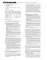
Start up
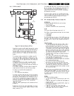
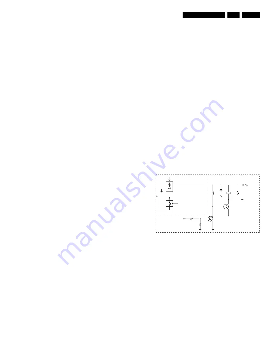
Figure 9-2 Start up circuitry
The mechanical "on/off" switch (item 1006) on the Front panel
drives IC7055. This is a "power distribution switch", used due
to the high switch-on current. It has internal overload and short-
circuit protections.
A single pole 5 V relay (item 1400) will switch the Receiver box
from "standby" to "on". It is controlled via the POWER_ON line.
The start up supply voltage of the control IC comes via the
standby supply. It is rectified (D6010), smoothed (C2025), and
clamped (D6008). Once the main supply is started, this voltage
is taken over by winding 6-8 of transformer 5003 and diode
D6007.
Normal operation
The working frequency of 40 kHz is determined by R3032 and
C2014. The output voltage is controlled by duty cycle
regulation. Output is on pin 3, which drives the FET. A current
will flow through transformer coil 3-4 (item 5003), FET 7000,
and sense-resistors R3012//R3013//R3014 to ground. The
energy stored in the primary winding during the on time is
delivered to the secondary windings during the "off" time.
The output voltages are rectified and buffered here.
1400
+5VSTBY
+5VSTB
1006
2/1
ON/OFF
POWER-ON
5/4
4
2/3
8/7/6
3
6
7055
3401
STANDBY
(FROM µP)
3403
6401
2
3
7401
TO BRIDGE
RECTIFIER (6000)
7402
3402
6402
CL36532021_001.eps
180303
FP
PS
Summary of Contents for F21RE
Page 7: ...Directions for Use EN 7 F21RE AB 3 3 Directions for Use ...
Page 8: ...Directions for Use EN 8 F21RE AB 3 ...
Page 9: ...Directions for Use EN 9 F21RE AB 3 ...
Page 10: ...Directions for Use EN 10 F21RE AB 3 ...
Page 11: ...Directions for Use EN 11 F21RE AB 3 ...
Page 12: ...Directions for Use EN 12 F21RE AB 3 ...
Page 13: ...Directions for Use EN 13 F21RE AB 3 ...
Page 14: ...Directions for Use EN 14 F21RE AB 3 ...
Page 15: ...Directions for Use EN 15 F21RE AB 3 ...
Page 16: ...Directions for Use EN 16 F21RE AB 3 ...
Page 17: ...Directions for Use EN 17 F21RE AB 3 ...
Page 18: ...Directions for Use EN 18 F21RE AB 3 ...
Page 19: ...Directions for Use EN 19 F21RE AB 3 ...
Page 20: ...Directions for Use EN 20 F21RE AB 3 ...
Page 21: ...Directions for Use EN 21 F21RE AB 3 ...
Page 22: ...Directions for Use EN 22 F21RE AB 3 ...
Page 23: ...Directions for Use EN 23 F21RE AB 3 ...
Page 24: ...Directions for Use EN 24 F21RE AB 3 ...
Page 25: ......
Page 114: ...Revision List EN 114 F21RE AB 11 11 Revision List First release ...


