background image

Service Modes, Error Codes, and Fault Finding

EN 7

FTP2.4E AB

5.

5.2.4

Error Codes

In case of non-intermittent faults, clear the error buffer before 
you begin the repair. This to ensure that old error codes are no 
longer present. Before clearing the buffer, write down the 
content, as this history can give you significant information. 
If possible, check the entire contents of the error buffer. In 
some situations, an error code is only the result of another error 
code and not the actual cause (e.g., a fault in the protection 
detection circuitry can also lead to a protection). 

There are various errors:

I

2

C device errors.

I

2

C bus errors.

Protection errors.

Errors not related to an I

2

C device, but of importance:

FEM (Falconic with Embedded Memory) (Error 26): 

at start-up, after initialisation of the PICNIC, the 
presence of the FEM can be checked.

Eagle (Error 27): 

at start-up, after initialisation of the 

PICNIC, the presence of the Eagle can be checked. 

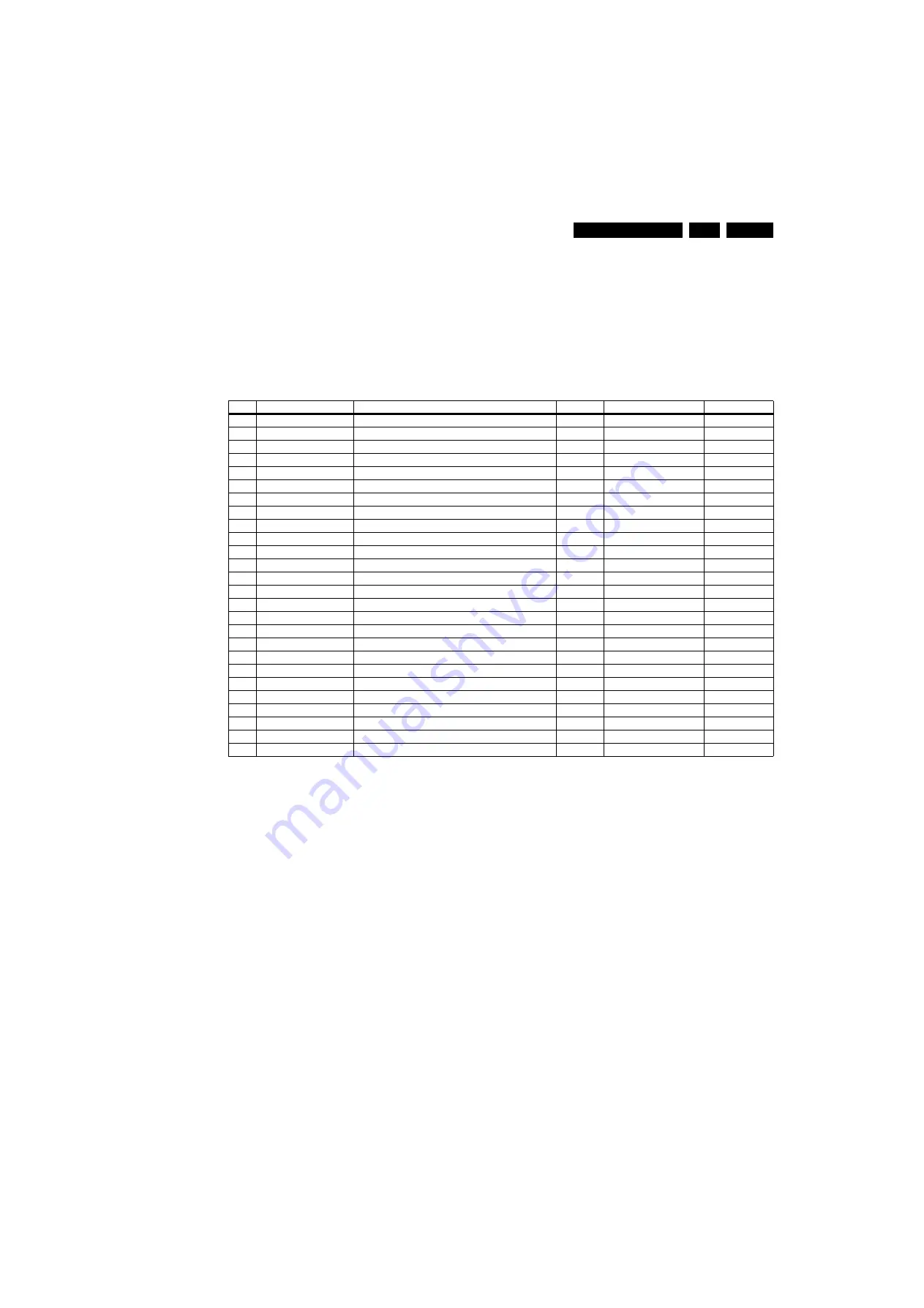
Table 5-1 Error Code Overview

Note

Error codes 1, 6, or 18 are protection codes. If one of the 
errors appears, there are supplies of some circuits that will 
be switched “off”. Also, in protection, the LED will blink the 
number of times equivalent to the most recent error code.

If error 3 or error 55 appears, depending on the software 
version, error 16 is also logged. Error 16 is a non existing 
error.

Depending on the SW version, it is possible that error 8 
(HIP error) is logged when switching off the TV with the 
mains.

Errors 65, 66, 67, 68, 69 and 99 are errors for the IBO 
module. Only errors 65 and 69 are possible errors. The 
other errors are for internal use.

Error Device

Description

Def. item

Def. Module indication Diagr.

1

M24Cxx

NVM, spontaneous blinking error 1

7011

-

B5a

3

SAA4978

PICNIC

7713

Feature Box

B3a

4

Supply 5 V

5V protection

-

+5V Supply

B5a

5

Supply 8 V

8V protection

-

+8V Supply

B5a

6

Slow  I

2

C bus blocked

Spontaneous blinking error 6

-

Slow I

2

C Blocked

-

7

Display

PDP error

-

Unknown

-

8

TDA932x

HIP High-end input Processor

7323

Chroma IF IO

B2

13

UV1318/...

Tuner protection

1T01

Tuner

B13a

14

MSPxxxx

ITT sound processor

7A02

Audio module

B6a

18

Fast I

2

C bus blocked

Spontaneous blinking error 18

-

Fast I

2

C Blocked

-

21

M62320

I/O Expander

7P56

Video Dual Screen

B15b

26

SAA4998

FEM (Falconic with Embedded Memory)

7760

+3V (FBX) Supply

B3b

27

T6TX5

Eagle 1C

7720

+3V (FBX) Supply

B3c

32

M29W400xx

Flash Ram (EPG)

7012

EPG Memory

B5a

35

T6TU5

Columbus

7752

Video Control

B3d

55

DC/DC converter

One of the voltages is not ok + protection error

-

Supply

-

65

IBO Module

Tuner error on “Digital Module"

-

TV module (IBO)

K6

66

IBO Module

Demodulation OFDM error on “Digital Module"

-

TV module (IBO)

-

67

IBO Module

DENC error on “Digital Module"

-

TV module (IBO)

-

68

IBO Module

EEPROM on “Digital Module"

-

TV module (IBO)

-

69

IBO Module

I

2

C error on “Digital Module"

-

TV module (IBO)

K1

76

Audio supply

Audio supply protection

-

Sound Output

-

83

TEA 6422

Source select matrix audio

7I17

Video source select

B14d

99

IBO Module

Digital Board IBEX terminal

-

TV module (IBO)

-

118

AD9883A

AD converter

7L01

HD

B19a

121

EPLD

EPLD error

7V01

Video control

B19d

Summary of Contents for FTP2.4E

Page 1: ... 4 Mechanical Instructions 3 5 Service Modes Error Codes and Fault Finding 5 6 Block Diagrams Testpoint Overviews and Waveforms Wiring Diagram 42 FHP Step 9 Wiring Diagram 50 SDI Step 10 Block Diagram Supply 11 Block Diagram Video 12 Block Diagram Audio 13 Block Diagram IBO Zapper 14 I2C IC s overview 15 Supply Lines Overview 42 FHP Step 16 Supply Lines Overview 50 SDI Step 17 Test Points and Wave...

Page 2: ...UART_TX Transmit k 2 Ground Gnd H 3 UART_RX Receive j DIGITAL AUDIO Cinch S PDIF Out Bk Coaxial 0 2 0 6 VPP 75 ohm kq 1 2 Chassis Overview Figure 1 2 PWB location photo from 50 SDI model 2 Safety Instructions Warnings and Notes See Service Manual FTP2 4E_AA 3122 785 15460 3 Directions for Use You can download this information from the following websites http www philips com support http www p4c ph...

Page 3: ...xecutions Follow the disassemble instructions in described order All photo s are made of the 50 SDI model however the 42 model will not deviate much from it Follow the disassemble instructions in described order Be aware that the internal gold coloured frame is made of conducting material So be cautious during electrical measurements 4 1 Cable Dressing 4 1 1 Chassis Figure 4 1 Chassis cable dressi...

Page 4: ...out the flat cable For re connection afterwards lift the black cable clamp of this connector 4 and put the flat cable back in Push down the black cable clamp of connector 1500 after the flat cable is plugged in 2 Disconnect white connector 1301 3 Disconnect the antenna cable 3 from the tuner on the IBO Zapper module Figure 4 4 Connector 1500 Figure 4 5 Remove IBO zapper module 1 Remove the torx sc...

Page 5: ...Application SW The application software version NOR version The NOR Flash image version Digital Frequency The digital frequency where the TV is tuned to Bit Error Rate The error rate is measured before the error correction algorithm circuitry This gives an impression of the signal quality Tuner AGC The tuner AGC value This gives an indication of the signal strength COFDM Lock Indication if the COF...

Page 6: ...ours When multiple errors occur errors occurred within a short time span there is a high probability that there is some relation between them 5 2 2 How to Read the Error Buffer Use one of the following methods On screen via the SAM only if you have a picture Examples 0 0 0 0 0 No errors detected 6 0 0 0 0 Error code 6 is the last and only detected error 9 6 0 0 0 Error code 6 was first detected an...

Page 7: ...ng off the TV with the mains Errors 65 66 67 68 69 and 99 are errors for the IBO module Only errors 65 and 69 are possible errors The other errors are for internal use Error Device Description Def item Def Module indication Diagr 1 M24Cxx NVM spontaneous blinking error 1 7011 B5a 3 SAA4978 PICNIC 7713 Feature Box B3a 4 Supply 5 V 5V protection 5V Supply B5a 5 Supply 8 V 8V protection 8V Supply B5a...

Page 8: ...Service Modes Error Codes and Fault Finding EN 8 FTP2 4E AB 5 Personal Notes E_06532_012 eps 131004 ...

Page 9: ...1 F_15740_013 eps 111005 AMBIENT LIGHT 2 AMBIENT LIGHT LAMPS RIGHT AMBIENT LIGHT LAMPS LEFT TUNER DVB KS IBO SUPPLY 0311 9P 1M30 2P3 1M52 9P 1M05 2P 1301 2P3 IBO ZAPPER MODULE K 1G50 31P 1M51 4P 1M46 11P 1M03 10P 1I11 32P 1M36 11P 1M07 5P 1M36 11P 1M37 11P 1M07 5P 1M20 12P 0345 6P 1M36 11P 3P 1402 SERVICE DIGITAL AUDIO OUT 1401 8220 1500 32P 1M20 12P TUNER MAIN 0307 20P 0306 6P 0308 2P 1M03 10P 1M...

Page 10: ...UNER DVB 1M52 9P 1301 2P3 1G50 31P 1M51 4P 1M46 11P 1M03 10P 1I11 32P 1M36 11P 1M07 5P 1M36 11P 1M37 11P 1M07 5P 1M20 12P 0345 6P 1M36 11P 3P 1402 SERVICE DIGITAL AUDIO OUT 1401 8220 1500 32P 1M20 12P TUNER MAIN 1M52 9P 1M02 7P 1736 2P3 1735 2P3 AL 1M12 3P AMBIENT LIGHT 2 1M08 4P 1M48 3P 1M10 4P 1M49 4P 1M11 11P 0345 6P 8131 K IBO ZAPPER MODULE LVDS CONN DISPLAY 31P 1M31 3P CN1M46 11P CN1M03 10P C...

Page 11: ...BY_SW 3396 3305 3303 3302 3316 3397 5V_STBY_SW 3364 5V_STBY_SW 12V_OVP 3389 6347 6362 3361 SUPPLY ON 6364 6340 6341 7389 7351 7352 3353 3344 3349 3202 VCC_GO 3224 FAN CONTROL 3225 8V6 DETECTION CIRCUIT 8V6 UNDER VOLTAGE PROT 7362 VCC_GO 2 5Vref VA VA 30V VS VS_UNSW 70 90V VB BIAS 12V 3363 7366 2 6378 5 7 7326 7327 6 3360 9V_STBY_SW 3388 3358 3332 3338 3333 3321 5225 7200 BSN304 7217 PSMN070 5121 1...

Page 12: ...WR OK PDP LCD PWR ON LAMP ON B3a B3c B19a Vref Href RSTR B3c B3c REF FALREF REFIN CLKP 7752 1 T6TU5XB 7753 MSN56V16160F 7TS SDRAM VA50 17 18 19 22 23 SCL_DVI SDA_DVI AV6 V 1I59 1I56 1I57 1I53 49 48 52 51 3 2 5 6 RX2 RX2 RX1 RX1 RX0 RX0 RXC RXC 24 C1 C2 C3 C4 GROUND 1 LOGIC SEPA SYNC DET 2 1 1 1 2 1 2 2 2 VD1 IN 12 VD2 IN HD S SIG DET 2 HD1 IN 24 HD2 IN 23 R OUT 21 R1 IN 1 R2 IN 7 20 VCC VD OUT 14 ...

Page 13: ... 19V 16V 17 7 5 13 8 10 19 16V 1 6 15W 8Ω 12 EN1 7701 TDA8925ST 19V 16V R 7706 7713 SOUND ENABLE POR DC PROT AUDIO SUPPLY SOUND ENABLE AUDIO L AUDIO R AUDIO SUPPLY PROT CIRCUIT 8VP DCPROT 19 16V TO 1002 A6 FHP SUPPLY OR CN1M02 SDI SUPPLY HEADPHONE OUT 5 12 4 14 3 13 7515 74HC4053 L FRONT IN SEL_FRONT_SC3 R FRONT IN FRONT L FRONT R SND CENTRE IN SNDL SEC IN SND CENTER IN POR PROT AUDIOSUPPLY_IBO SO...

Page 14: ...NTROL CONTROL LINES A_MD 0 7 A_MDO 0 7 LATCH 7701 74LVC573ADB 68P PCMCIA CONN MIU_ADDR 8 14 PCMCIA A 8 14 CONTROL LATCH 7702 74LVC573ADB PCMCIA D 0 7 CONTROL BUS TRANS CEIVER 7703 74LVC245A 1 34 35 68 FROM MAIN TUNER LC4 X OR JL2 1 38 37 36 35 33 FE_LOCK 25 8 10 5 13 AGC XTAL 8 6 8 6 4 54 X IN 5V 5V 5V 5 6 7 7602 M24C256 EEPROM INVERTER 4 2 2 4MHz_MOJO INVERTER 7606 74AHC1GU04GW 7605 74AHC1GU04GW ...

Page 15: ...SDA EPLD 3826 3827 7713 SAA4978H PICNIC 3758 SDA D SDA CL 9817 9818 9815 9816 9757 9755 SN DA ERR 27 ERR 26 DVI INPUT CONNECTOR SDA DVI SCL DVI 3I49 3I46 7I18 SII907BCQ DVI RECEIVER 3002 3001 AL CL 3A17 3A17 7P56 M62320FP I O EXPANDER ERR 21 SDA S 9E57 9E58 RES RES 3E69 3E70 3L06 3L03 ERR 118 57 56 7E23 AD9883AKST A D CONVERTER 3E18 3E19 ERR 118 3E18 3E18 AL DA IN ERR 35 9I06 9I05 3IB3 3IB1 SDA DI...

Page 16: ...A EAn 3C01 B5a 3400 8V_VDP B14e B15c B19b B20 B21 B14e B21 B14e B4 B3e B3e B3e B3e B3e B3e B3e B3e B3e B3e B3e B3e B3e B3e B3e B3e B3e B3e B3e B3e B3e B3e B3e B3e B3e B3e B3e B3e B3e B3e B12 B6a B2 B14e B14e B21 B5c B2 B5c B14e B2 B5a B21 B21 B14b B21 B6a B6a B6a B6a B6b B21 B14e B21 B21 B21 B21 B21 B21 B21 B14b B21 B12 B21 B21 B15a B21 B15b B12 B21 B12 B19a B19b B19b B21 B19b B12 B13c B21 B3e B5a...

Page 17: ...5ED 2V5EC 1V5EA 1V5EB 2V5EB 2V5EA 3V3EA 3V3EB 5V2Pr 3V3EC 3V3ED 3V3FB 3V3FA 1V8FA 1V8FA 3V3_DCDCFBXA 1V5_FBXA 3V3_FBXB 5V2Pr 2V5_FBXA 3V3PA 8VPA 3V3Pr 3V3PB 3V3PC 3V3GA 3V3FB 3V3FA 1V8FA 5VS 8V 5416 5V_VDP 3402 1V8FA 3V3_DCDCFBXA 1V5_FBXA 3V3_FBXB 5V2Pr 2V5_FBXA 3V3PA 8VPA 3V3Pr 3V3PB 3V3PC 3V3GA 8V_VDP 8VP 5VS 8V 5V_VDP 5VCOM 8V_CON 33V 8V 5Y06 5V 5Y15 11V 5Y02 5V2 STBY 5Y07 5Y03 5V 5Y00 9Y15 9V ...

Page 18: ...V 1 of 1534 12VA 11 7V 2 of 1004 On bottom side On bottom side 7600 7700 7100 1600 General RESET Tuner I2C bus pin 8 9 of 1600 5V no command 3625 3629 Local I2C bus idem bus TV 5V 2 7307 5Vclean 2 7308 1V2 MOJO 5101 5102 1V8FE 2 7302 3V3 S 7311 IRQ 4 of 1206 5V start with 0V after command FE_LOCK 3621 3 1V fixed 0V without reception ...

Page 19: ...3 6 33R 3157 1 3 6 33R 3156 3 2 7 33R 3159 3 33R 3157 2 33R 3158 2 2 7 3V3clean 2104 100n 2108 100n 3V3_MOJO 1 2 22R 3134 1106 B2B PH K 3146 100R 10K 3119 F131 4 5 1V2_MOJO 4 5 33R 3157 4 2 7 33R 3158 4 4 5 33R 3156 2 33R 3156 4 33R 3159 2 2 7 26 28 4 6 8 10 12 14 16 18 ROW_2 1100 2 2 20 22 24 3 5 7 9 11 13 15 17 FTSH 114 01 L DV 1 19 21 23 25 27 ROW_1 1100 1 FTSH 114 01 L DV 10K 3155 F133 2 20 3 ...

Page 20: ... HEATSINK HEATSINK 0009 0008 HEATSINK 2211 100n 4215 4200 HEATSINK 0007 2202 100n 3V3_NOR48 I203 I200 470R 3212 I205 3209 100R 3210 100R 3V3_NOR48 3V3_NOR48 100n 2207 5V 3V3_NOR48 4212 3V3_NOR48 470R 3204 5200 F201 3V3 I211 I206 5203 I210 100n 2209 4214 11 3V3 44 30 32 13 28 15 12 37 14 27 46 34 36 39 41 43 45 33 35 38 40 42 21 20 19 18 8 7 47 26 29 31 3 2 1 48 17 16 9 23 10 22 7200 M29W320DT 25 2...

Page 21: ...11 2308 SUPPLY_GND 470p 47K 3329 SUPPLY_GND SUPPLY_GND 12V 3312 1R0 I306 I301 2335 100u 16V 6304 SUPPLY_GND SUPPLY_GND SS14 5304 10u 2331 4n7 SUPPLY_GND I310 3311 I331 3319 1R0 F317 I326 2332 100u 25V 3320 1R0 3313 1R0 SUPPLY_GND 2326 470n F315 6 1K0 3306 8 GND 4 IS 7 SWC 1 SWE 2 TIMC 3 VCC REGULATOR REFERENCE OSC IPK Q R S 7305 MC34063AP1 CIN_NEG 5 DCOL F308 3V3 100n 2312 1V2_MOJO 4302 2303 4n7 3...

Page 22: ...F423 F10 F424 F10 I402 F6 I403 F6 I404 E7 I405 F9 I406 F9 I416 B7 I417 B8 5V1 3V3 0V 4V5 K1 K1 USB RES RES RES RES RES RES 100MHz I418 B6 I419 B8 I420 B6 I421 B9 K1 K1 K1 3V3 1V6 1V K1 K1 I403 2406 100u 6 3V 3V3 4402 100n 2413 7402 BC847B I405 100R 3414 2411 100n 3403 10K F409 1400 I402 1401 YKC21 3416 1 3 2 560R 3404 BZX384 C5V1 6400 330p 2415 1K0 3405 3406 1K0 F407 5401 33R F408 3420 3V3 68R 340...

Page 23: ... K1 I538 E4 I541 G5 I542 G10 I543 D5 I544 E5 I545 E5 I546 E6 I547 F9 I548 E5 I549 F5 I550 F8 I551 F9 I552 G8 I553 G9 I554 G9 RES RES RES RES RES RES RES 2V1 K1 1K0 3564 100K 3563 100n 2544 4n7 2515 12V_A 560R 3532 I533 7510 BC847B I549 75R 3547 68K 3510 I501 75R 3519 2531 390p BC847B I502 7501 2 BC857B 7500 11 7 6 13 4 14 16 12 15 5 UDA1334ATS 1 3 9 8 10 7502 DAC Φ 5504 F502 I537 4506 3572 150R I5...

Page 24: ...01 2 5 6 7 8 5Vclean 100n 2628 5 4 2620 100n 7606 74AHC1GU04GW 2 3 1 100R 3606 I631 3V3 3V3 5601 F603 100R 3630 VSS6 VSS7 52 VSS7 63 VSSA_ADC VSSA_ADC 56 VSSA_OSC VSSA_OSC 58 VSS_PLL_ADC VSS_PLL_ADC XIN XIN 54 XOUT 55 XOUT VDDI18_4 VIM 61 VIM VIP 62 VIP VSS1 7 VSS1 VSS2 15 VSS2 VSS3 VSS3 24 VSS4 29 VSS4 VSS5 40 VSS5 VSS6 45 VDDA18_PLL 60 VDDA33_ADC VDDA33_ADC 19 VDDE33_1 VDDE33_1 34 VDDE33_2 VDDE3...

Page 25: ...61 I722 10K 3710 10K 3706 I707 3V3_STV PCMCIA_AVCC 3V3_STV PCMCIA_5V 3703 4 33R I736 I760 I752 10K 3704 10K 3720 I754 I769 I773 I770 3V3_STV I720 F700 I709 10K 3715 3V3_CORE I749 3721 10K 97 WR STR 16 I700 VCC PROC 109 VCC TSI 51 VCC TSO 64 VCCEN 70 WAITA_ 122 WAITB_ 121 WAIT ACK 15 WE_ 31 SDA 30 TCK 11 TDI 38 TDO 10 TMS 65 TRST_ 8 VCC CORE 36 100 RD DIR 17 REG_ 123 RESET 34 RSTA 120 RSTB 119 SA0 ...

Page 26: ...26 FTP2 4E AB 7 Circuit Diagrams and PWB Layouts Layout IBO Zapper Top Side F_15740_008 eps 041005 3139 123 5906 4 ...

Page 27: ...Circuit Diagrams and PWB Layouts 27 FTP2 4E AB 7 Layout IBO Zapper Bottom Side F_15740_009 eps 041005 3139 123 5906 4 ...

Page 28: ...83 D6 I190 E6 I193 E8 I194 F8 I195 F8 I196 G9 I197 H9 I198 H9 I171 TO IBO ZAPPER PANEL only for 42 FHP TO 1M05 I141 C9 GND HOT I112 2113 47p 3102 1K2 I150 3999 1K0 I101 I127 I132 GND HOT F100 5112 80R 330K GND HOT I197 3138 F120 GND HOT 3109 3529 150K 390R I117 I105 F102 I114 220p 2104 68R 25V 100u 3148 5102 82u 2102 10K 3149 6104 BZX384 C27 I168 I123 GND SSP GND HOT 390R 3110 I115 PDZ3 9 B 6122 5...

Page 29: ... Panel Bottom Side F_15740_012 eps 051005 3104 303 5002 2 2103 B1 2104 A1 2105 B1 2109 D1 2110 A1 2111 A1 2112 A1 2113 A1 2123 A1 2142 E1 2143 E1 2144 A1 2145 A1 2149 C1 2153 C1 2159 B1 2162 B1 2536 D1 2537 D1 3102 B1 3103 B1 3104 A1 3106 A1 3107 A1 3109 A1 3110 A1 3112 A1 3114 C1 3121 D1 3123 D1 3124 D1 3125 A1 3127 A1 3128 A1 3129 A1 3137 E1 3138 B1 3145 A1 3146 A1 3147 A1 3148 A1 3149 A1 3150 A...

Page 30: ...30 FTP2 4E AB 7 Circuit Diagrams and PWB Layouts ...

Page 31: ...ntended for use in combination with an analogue TV chassis 9 3 Block Diagram IBO Zapper Module Figure 9 1 Block Diagram IBO zapper module G A T J E U I M L A T X M A R D S R I B S U 1 C 2 I T E S E R 2 3 2 S R X U M E D R C S E D o i d u A 1 G E P M r e d o c e d o e d i V 2 G E P M r e d o c e d U P C O J O M x x 3 8 x n p TS in I2C0 SmCard1 SmCard0 SPDIF I2S Analog Video Out M A R D S B M 6 1 H ...

Page 32: ...s sent to the HIP video switch input pin 23 The signal then appears on one of the outputs of the HIP video switch pin 34 and is passed on via buffer 7415 to pin 19 of SCART 2 which is the CVBS monitor output For further details see the manuals of the original TV sets on which the various models of IBO zappers are based 9 6 3 Audio Outputs The MOJO has two audio output interfaces SPDIF Out The SPDI...

Page 33: ... CBA Circuit Board Assembly also called PCB or PWB CI M Common Interface Module E g PCMCIA slot for a CAM in a set top box ComPair Computer aided rePair A tool for diagnosing a TV through a PC controlled interface COFDM Coded Orthogonal Frequency Division Multiplexing A multiplexing technique that distributes the data to be transmitted over many carriers CSM Customer Service Mode CVBS Composite Vi...

Page 34: ...B PCMCIA Personal Computer Memory Card International Association PLL Phase Locked Loop Used for example in FST tuning systems The customer can directly provide the desired frequency Progressive Scan Scan mode where all scan lines are displayed in one frame at the same time creating a double vertical resolution PWB Printed Wiring Board also called PCB or CBA QAM Quadrature Amplitude Modulation modu...

Page 35: ...2 PNx831x architecture and data paths Block Diagram Video decoder Audio decoder MPEG system processor Background color Display Graphics OSD Cursor Mixer unit DENC Priority int ctrl USB host GPIO Infrared RS232 UART0 Boot I2C unit1 RS232 UART1 ISO7816 UART Analog video CCIR 656 CPU PR1910 PI Bridge DMA SDRAM interface Central Data Unit MIU 3 L P V D s u B 2 L P V D Slow PI Bus 60 MHz Fast PI Bus 12...

Page 36: ...ding CHANNEL DECODER VBER CBER CPT_UNCOR MPEG TS parallel CHANNEL ESTIMATION AND CORRECTION OFDM Spectrum Confidence I Q Carrier Recovery VIP XOUT Time Recovery ACI Filtering Digital AGC Dynamic TimeShift FFT 2K 8K Coarse Time Estimator Dual AGC Σ AGC_IF ANALOG Time Interpolation Frequency Interpolation Partial Channel Estimation CPE calculation Channel Correction Confidence Calculation Outer Forn...

Page 37: ...2238 586 59812 100nF 20 50V 0603 2610 2238 586 59812 100nF 20 50V 0603 2611 2238 586 59812 100nF 20 50V 0603 2612 2238 586 59812 100nF 20 50V 0603 2613 2238 586 59812 100nF 20 50V 0603 2614 4822 124 80151 47µF 16V 2615 2238 586 59812 100nF 20 50V 0603 2617 2238 586 59812 100nF 20 50V 0603 2618 2238 586 59812 100nF 20 50V 0603 2619 2238 586 59812 100nF 20 50V 0603 2620 2238 586 59812 100nF 20 50V 0...

Page 38: ...2 10µH 10 5305 2422 536 00548 100µ 5306 4822 157 10452 10µH 10 5309 3198 018 90050 Bead 1kΩ at 100MHz 5401 4822 157 11499 Bead 60Ω at 100MHz 5502 4822 157 11499 Bead 60Ω at 100MHz 5504 4822 157 11499 Bead 60Ω at 100MHz 5505 4822 157 11499 Bead 60Ω at 100MHz 5507 4822 157 11499 Bead 60Ω at 100MHz 5508 4822 157 11499 Bead 60Ω at 100MHz 5511 3198 018 52280 2 2µF 10 1008 5512 3198 018 52280 2 2µF 10 1...

Page 39: ... 6108 4822 130 80622 BAT54 6109 4822 130 11522 UDZ15B 6112 9322 202 75687 BYW29FP 200 6114 5322 130 31938 BYV27 200 6116 3198 020 55680 BZX384 C5V6 6117 9340 548 71115 PDZ33B 6118 9340 548 71115 PDZ33B 6120 4822 130 11397 BAS316 6121 4822 130 11397 BAS316 6122 9322 129 34685 BZM55 C3V9 6123 4822 130 11416 PDZ6 8B 6142 4822 130 80622 BAT54 6144 4822 130 11397 BAS316 6147 9322 208 44685 BZG05C6V8 61...

Page 40: ...Revision List EN 40 FTP2 4E AB 11 11 Revision List Manual xxxx xxx xxxx 0 First release ...

Reviews: