background image

6-2

6-2

This assembly drawing shows a summary of all possible versions. For components used in a specific version see schematic diagram and respective parts list.

3139 113 3514 pt4  dd wk0310

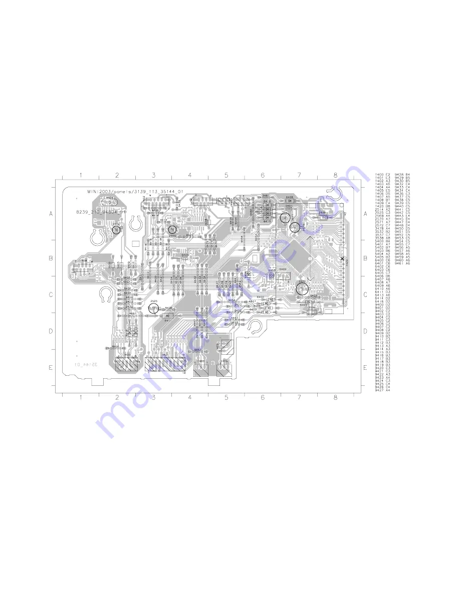
DISPLAY BOARD - COMPONENT LAYOUT

Summary of Contents for FW-M589

Page 1: ...lay Board 6 ECO6 Tuner Board Systems Non Cenelec 7A Systems Cenelec 7B PWR303 Module UCD 200 250W 8 AF12 Board 9 5DTC Module MP3 Version 10 Set Mechanical Exploded view parts list 11 Copyright 2005 Philips Consumer Electronics B V Eindhoven The Netherlands All rights reserved No part of this publication may be reproduced stored in a retrieval system or transmitted in any form or by any means elect...

Page 2: ...ems Cenelec x USB PC LINK x x x Game Port Video Audio L Audio R x x x VERSION VARIATIONS Type Versions FW M589 Features Board in used 30 x MAINS BOARD AMPLIFIER UCD BOARD 1 MAINS SOCKET BOARD VIDEO OUT CINCH BOARD TUNER BOARD AF11 BOARD FRONT DISPLAY BOARD VU METER BOARD R VU METER BOARD L FRONT CONTROL BOARD GAME PORT BOARD USB SOUND AGENT BOARD USB LED BOARD IR EYE BOARD ECO POWER BOARD HEADPHON...

Page 3: ...utput power 6 Ω 1kHz 10 THD L R 2 x 200W RMS 21 22 30 2 x 160W FTC 37 Frequency response within 3dB 63Hz 16kHz MAX Sound On Off Game Sound Speed Punch Blast Off Dynamic Bass Boost DBB DBB 1 2 3 Off Digital Sound Control DSC Jazz Rock Pop Optimal Virtual Ambience Control VAC Cyber Arcade Hall Cinema Concert Input sensitivity Aux in at 1kHz 640mV 2dB Game Port at 1kHz 310mV 2dB USB at 1kHz 830mV at ...

Page 4: ...7122 707 89001 Tuner AM MW LW To avoid atmospheric interference all AM measurements have to be carried out in a Faraday s cage Use a bandpass filter or at least a high pass filter with 250Hz to eliminate hum 50Hz 100Hz RF Generator e g PM5326 Ri 50 Bandpass 250Hz 15kHz e g 7122 707 48001 LF Voltmeter e g PM2534 DUT RF Generator e g PM5326 S N and distortion meter e g Sound Technology ST1700B Use a...

Page 5: ...ogic Test Disc 4822 395 10216 ESD Equipment Anti static table mat large 1200x650x1 25mm 4822 466 10953 Anti static table mat small 600x650x1 25mm 4822 466 10958 Anti static wristband 4822 395 10223 Connector box 1MΩ 4822 320 11307 Extension cable to connect wristband to conn box 4822 320 11305 Connecting cable to connect table mat to conn box 4822 320 11306 Earth cable to connect product to mat or...

Page 6: ...ectrostatische ontladingen ESD Onzorgvuldig behandelen tijdens reparatie kan de levensduur drastisch doen verminderen Zorg ervoor dat u tijdens reparatie via een polsband met weerstand verbonden bent met hetzelfde potentiaal als de massa van het apparaat Houd componenten en hulpmiddelen ook op ditzelfde potentiaal I AVVERTIMENTO Tutti IC e parecchi semi conduttori sono sensibili alle scariche stat...

Page 7: ...the stripped portion of the speaker wire into the terminal as shown on page 10 Notes Ensure that the speaker cables are correctly connected Improper connections may damage the system due to short circuit Do not connect more than one speaker to any one pair of speaker terminals Step 3 Connecting to PC via USB cable Use the supplied USB cable to connect the system to your personal computer s USB por...

Page 8: ... to the GAMEPORT video and audio inputs respectively refer to Connections Connecting to game console 2 Connect your TV s video input to the VIDEO OUT CVBS on the rear panel 3 Connect all the AC power cord to the power outlet Starting operation 4 Turn on the TV and set to the correct video in channel The TV s video input channel may be called AUX iliary IN AUDIO VIDEO A V IN EXT 1 etc These channel...

Page 9: ...music sources CD TUNER USB PC LINK or AUX MODE GAME SOUND Selects different type of equaliser setting for Gameport SPEED PUNCH or BLAST Connect the USB cable between the system and PC s USB port GAME VOLUME Adjusts the game s output volume level VIDEO Use a video cable to connect to your game console s video output AUDIO L AUDIO R Use an audio cable to connect to your game console s left right aud...

Page 10: ...omputer to the folder where audio files are stored Check the box Also Add Tracks from Subfolders to add all tracks in the current folder and all subfolders 3 Click the Select All button to select all the files in the current and all subfolders 4 Click Add Files will be added to My Library To create a Playlist 1 Drag and drop files or folders with music files from anywhere on your computer or My Li...

Page 11: ...nhance the quality of MP3 Music playback via USB PC Link 1 Philips Sound Agent 2 will be automatically launched if USB PC Link is selected 2 Press DSC PRESET or VAC REVERB to select different Preset or Reverb sound effect 3 For more details about using Philips Sound Agent 2 features on your PC please refer to the User Manual in the supplied CD ROM or the Help menu Notes Philips Sound Agent 2 minim...

Page 12: ...mode If the signal is too weak adjust the antenna or connect an external antenna for better reception Increase the distance between the system and your TV or VCR Insert a disc Load in the disc with the labeled side facing up Replace or clean the disc see Care and safety information Use a finalised CD R W or a correct format disc Remove and reconnect the AC power cord and switch on the system again...

Page 13: ... 3 To loosen the Panel Front Display pos 120 you have to press in the correct direction and position as shown in Figure 1 and Figure 2 Once the Panel Front Display is loosen remove it out in the direction as shown in Figure 3 4 Loosen 4 screwsA see Figure 4 and Figure 16 to remove the 5DTC Module pos 1105 2 screws on the front 2 screws on the rear Note For information on the Emergency opening of t...

Page 14: ...er 2 pos 136 and loosen 2 screws H to remove the VU Meter Right Board pos 1107 D from the Bracket VU Meter 2 7 Loosen 3 screws J see Figure 12 to remove the Bracket VU Meter 1 pos 129 and loosen 2 screws K to remove the VU Meter Left Board pos 1107 C from the Bracket VU Meter 1 8 Loosen 2 screws L see Figure 13 to remove the USB PC LINK Board pos 1104 9 Loosen 9 screws M see Figure 13 and loosen t...

Page 15: ... 1001 B DISMANTLING INSTRUCTIONS Note The flex cables are very fragile care should be taken not to damage them during repair After repair be very sure that the flex cables are inserted properly into the flex sockets before encasing otherwise faults may occurs 5 Loosen 4 screws W see Figure 16 and 2 catches C3 see Figure 7 to remove the Panel Rear pos 256 by sliding it out towards the rear see Figu...

Page 16: ...Service position A Service position B Service position C 2 4 2 4 DISMANTLING INSTRUCTIONS ...

Page 17: ...pressed No Display shows and switch all LEDs off with 2 3 deflection on VU meter Right 2 3 deflection on VU meter Left Y N Y N N PLAY Button pressed PLAY Button pressed PLAY Button pressed ADC TEST Display shows ADC1 Value for ADC1 Input Line IoSA2 Display shows ADC2 Value for ADC2 Input Line IoSA1 Y Y N 9 Button pressed ADC Test is used for checking the ADC inputs to the microprocessor The displa...

Page 18: ...tain time The tray could not enter the inside position and is opening again This can happen if the tray is blocked such that it cannot go fully inside or if the 5DTC control module is defective and never closes The tray could not reach the outside position and is stopped at its blocked position This can happen if the tray is blocked such that it cannot go fully outside or if the 5DTC control modul...

Page 19: ...6dBA 3 5dBA A S W OUT CCT CCT LOW_PW_SPLY A Signal S N AT 500mW HEADROOM 1 THD WRT TO LEVEL AT MAX VOL 500mV SA_OUT Vkk 9V1 A Mute2 Vkk TUNER IS Interface Audio Mute CMOS A A D A 9V 5V From other 5DTC Mute1 LEVELS AT MAX VOL D REG 12V_A CMOS Proc Mute_SW_FR H P Amp 2 50V 85dBA 3dB AUX 640mV A A VREF CON 200mV 76dBA 16dB 1 90V 67dBA 3dB Mute A REG 5V6 VKK 2 1V Mute_SW A MIC A DIG Line Out A A 125mV...

Page 20: ...ower Booster Out 1531 SUPPLY_GND V EN22 EN11 SMF 1P 280 1P STO 8 1107 1 GND_D_COAX SHIELD TRAY_I2C_SCL TU_CLK 4 15 5V_CD 8 GND_A 8405 IIC_SUSP N C 1 EH TOP ENTRY HP_RIGHT GND_A 1830 HR 03p 180 3p OE GND_A TU_RIGHT CD_SH_STR FREQ MODE SEL SPK_GND GND_D V REF 5DTC MP3 IR Receiver 1860 HR 3p 280 3p OE DQSY 19 TU_STEREO 8601 F2 CD_SH_DATA FFC BD 04p 180 F uAC_READY Key2 SICL SW_INFO 1805 1 Out 19 GM_R...

Page 21: ...1842 A3 2841 A2 2843 A2 2844 A3 5840 B2 5841 B2 5842 A3 9840 A3 1 2 3 4 1842 RT 01T 1 FE BT VK N 1840 9840 5842 2u2 HP HP 2841 22n 2844 100n 2843 22n 5841 2u2 2u2 5840 1841 9 8 7 1 2 3 4 5 6 HP_DET HP_LEFT HP_RIGHT HP TC38 3139 118 56720 8239_210_94764 for 3513 pt4 dd wk0310 Note Some values may varies see respective parts list for correct value Provision HEADPHONE This assembly drawing shows a su...

Page 22: ...ONTROL BOARD COMPONENT LAYOUT This assembly drawing shows a summary of all possible versions For components used in a specific version see schematic diagram and respective parts list 3139 113 3513 pt4 dd wk0310 ...

Page 23: ...3 CONTROL BOARD CHIP LAYOUT This assembly drawing shows a summary of all possible versions For components used in a specific version see schematic diagram and respective parts list 3139 113 3513 pt4 dd wk0310 ...

Page 24: ...3 180R 470R 3697 GND_A 16V 100u 2615 470R 3647 4K7 3709 Gnd 3664 220R GND_B 7 4 8 9 1 3 6 5 3660 EWCY8AF20A24 20K 2 1659 GND_B Gnd Gnd Gnd GND_A 47K 3656 1664 Gnd 3683 Gnd 1K 7650 BC847B 1K 3684 BC847B 7605 10K 3692 GND_B 6622 100p 2636 6624 Gnd 1658 1651 3691 10K GND_B 3655 6623 2K7 3681 3698 470R 1672 GND_B GND_A 220R 3706 3680 1K2 2646 2u2 50V 2645 2u2 50V GND 5 IN 2 INL 1 INR 3 OUTL 7 OUTR 6 S...

Page 25: ...C4 2891 B2 2892 B3 2894 A2 2895 A3 2896 B4 2897 B4 3890 A2 3891 A2 3892 A3 3893 B3 2891 680p YKC21 4503N 1891 2895 470p 2890 1897 3893 1K2 3892 1K2 3 2 1 2897 100p RT 01T 1 100p 2896 10K 3890 3891 10K 1 2 3 220n YKC21 3826 1890 3 2 1 1893 EH S YKC21 3564 1892 3 2 1 HR 1894 1 2 470p 2892 680p 2894 GND_video 3139 118 56720 8239_210_94824 for 3513 pt4 dd wk0310 Note Some values may varies see respect...

Page 26: ...139 118 56720 8239_210_94814 for 3513 pt4 dd wk0310 Note Some values may varies see respective parts list for correct value VU METER LEFT To Front Display Board This assembly drawing shows a summary of all possible versions For components used in a specific version see schematic diagram and respective parts list 3139 113 3513 pt4 dd wk0310 This assembly drawing shows a summary of all possible vers...

Page 27: ... VUMeter 5V6 5V6 3139 118 56720 8239_210_94844 for 3513 pt4 dd wk0310 Note Some values may varies see respective parts list for correct value VU METER RIGHT This assembly drawing shows a summary of all possible versions For components used in a specific version see schematic diagram and respective parts list 3139 113 3513 pt4 dd wk0310 This assembly drawing shows a summary of all possible versions...

Page 28: ...e schematic diagram and respective parts list 3139 113 3513 pt4 dd wk0310 A B 1850 A1 3850 B1 6850 B2 1 2 1 2 A B EH B 1850 1 2 LTL 8166FTNN 6850 3850 820R 3139 118 56720 8239_210_94784 for 3513 pt4 dd wk0310 Note Some values may varies see respective parts list for correct value USB LED This assembly drawing shows a summary of all possible versions For components used in a specific version see sc...

Page 29: ...063W 3657 4822 051 30472 4k7 5 0 062W 3658 4822 051 30472 4k7 5 0 062W 3659 4822 051 30472 4k7 5 0 062W 3660 4822 101 11904 POTM 20KX2 20 0 025W 3661 4822 051 30103 10k 5 0 062W 3662 4822 051 30103 10k 5 0 062W 3663 4822 051 30151 150R 5 0 062W 3664 4822 051 30221 220R 5 0 062W 3665 4822 051 30271 270R 5 0 062W 3666 4822 051 30391 390R 5 0 062W 3667 4822 051 30561 560R 5 0 062W 3668 4822 117 12968...

Page 30: ...804 BC817 25 7608 4822 130 42804 BC817 25 7609 4822 130 42804 BC817 25 7610 4822 130 42804 BC817 25 7620 4822 209 33985 TDA8579T N1 7650 5322 130 60159 BC847B 7800 9322 185 97667 IR Receiver TSOP4836ZC1 7810 5322 130 60159 BC847B 7811 5322 130 60159 BC847B 7812 5322 130 60159 BC847B 7813 5322 130 60159 BC847B 7814 5322 130 60159 BC847B 7830 5322 130 60159 BC847B 7831 5322 130 60159 BC847B 7832 532...

Page 31: ... P4 P5 P6 P7 P8 P9 P10 P11 P12 P13 P14 P15 P16 P17 2G a h j p k b f m g c e r n d 1G 3G a h j p k b f m g c e r n d 4G a h j p k b f m g c e r n d 5G a h j p k b f m g c e r n d 6G a h j p k b f m g c e r n d 7G a h j p k b f m g c e r n d col Dp 8G a h j p k b f m g c e r n d 9G a h j p k b f m g c e r n d 10G A1 A2 A3 A4 A5 11G FTD DISPLAY PIN CONNECTION 2G 9G col Dp b f h g m a j k e r p n c d ...

Page 32: ...his assembly drawing shows a summary of all possible versions For components used in a specific version see schematic diagram and respective parts list 3139 113 3514 pt4 dd wk0310 DISPLAY BOARD COMPONENT LAYOUT ...

Page 33: ...3 This assembly drawing shows a summary of all possible versions For components used in a specific version see schematic diagram and respective parts list 3139 113 3514 pt4 dd wk0310 DISPLAY BOARD CHIP LAYOUT ...

Page 34: ...581 1K0 3557 220R 47p 2556 1 2 GND B 1u0 2566 100n 2543 2537 1u0 10K 3472 5404 AT 51 10u 2569 100p 2504 1409 440053 1 2 3 3520 3566 220R 47K 47p 2551 1K0 3450 5 6 7 9 220p 2580 1402 FE BT VK N 1 10 2 3 4 2552 47p 47u 2570 3410 22R 2509 100n 2K7 3529 4K7 3409 10K 3849 3466 1K0 1K0 3401 2505 100p 2506 100p FE BT VK N 14071 2 3 4 5 2K7 3511 3436 1K0 100p 2548 3523 470K 2553 47p 2508 47n 220R 3482 1 1...

Page 35: ... 40248 10uF 20 63V 2570 4822 124 12233 47uF 20 25V 2571 4822 124 12233 47uF 20 25V 2572 3198 028 44790 47uF 20 35V 2574 4822 122 33761 22pF 5 50V 2575 4822 122 33761 22pF 5 50V 2576 4822 122 33761 22pF 5 50V 2577 4822 122 33761 22pF 5 50V 2578 2238 586 59812 100nF 50V 2579 4822 126 13883 220pF 5 50V 2580 4822 126 13883 220pF 5 50V 2581 4822 126 13883 220pF 5 50V 2582 4822 126 13883 220pF 5 50V 258...

Page 36: ...822 051 30102 1k 5 0 062W 3431 4822 051 30102 1k 5 0 062W 3432 4822 051 30102 1k 5 0 062W 3433 4822 051 30102 1k 5 0 062W 3434 4822 051 30102 1k 5 0 062W 3435 4822 051 30102 1k 5 0 062W 3436 4822 051 30102 1k 5 0 062W 3437 4822 051 30102 1k 5 0 062W 3440 4822 051 30153 15k 5 0 062W 3441 4822 051 30103 10k 5 0 062W 3442 4822 051 30474 470k 5 0 062W 3443 4822 051 30684 680k 5 0 062W 3444 4822 051 30...

Page 37: ... 6 5 43 C D 450kHz 450kHz 450kHz 20 75kHz VStabA VStabB VStabB VStabA VStabB 10 7 MHz 10 7 MHz 35 9 Vdd Vcc1 7 23 VStabA VStabB 38 34 22 Vcc2 8 ECO6 Systems 140499 LF filter RDS MPX RDS MPX stereo clock data enable Version 1120 1 8 FM Frontend AM Frontend AM FRAME AERIAL B 1103 1101 1102 A FM MPX buffer ampl 5 Discriminator 10 7 MHz Vdd Vcc1 Vcc Vcc2 AM RF AM Osc FM Osc FM RF FM IF 1 FM IF 2 AM IF...

Page 38: ...1n 3134 22K 6105 2 HN1V02H 100n 2163 T141 7KL 1K 3144 5102 3157 100K T109 470R 3153 2130 22n 220R 3105 3142 100K 3167 120R 33p 2149 2K2 3145 1132 C PAD T103 T111 2164 470n T102 2140 15p 2139 2138 2u2 82p 2133 1u 3103 8K2 T120 4p7 2154 3156 1101USA YKD21 100K 2161 100n 5119 2119 10p T142 5123 11p 2106 3172 6106 BAS216 100n 2165 5K6 3154 3155 220R 330R 2124 33K 3176 22n WRITE EN 5114 7P MUTE P0 P1 P...

Page 39: ...riginal frame antenna has to be used 2 RC network serves for damping the IF filter while adjusting the other one 4 MW has to be aligned before LW Waverange Input frequency Input Tuned to Adjust Output Scope Voltmeter FM 87 5 108MHz 65 81 74 87 5 108MHz FM MW version 9kHz grid 531 1602kHz as low as possible ECO6 System non Cenelec stage 3 120900 TUNER BOARD ECO6 Systems non Cenelec componentside vi...

Page 40: ...10 63V RDS only RESISTORS 3101 4822 051 20333 33kΩ 5 0 1W 3102 4822 117 10837 100kΩ 1 0 1W 3103 4822 051 20822 8 2kΩ 5 0 1W 3104 4822 117 13577 330Ω 1 0 1W 3105 4822 117 11503 220Ω 5 0 1W 3132 4822 051 20479 47Ω 5 0 1W 3134 4822 051 20223 22kΩ 5 0 1W 3141 4822 117 11148 56kΩ 1 0 1W 3142 4822 100 12159 TRIMPOT 100kΩ RESISTORS 3143 4822 051 20223 22kΩ 5 0 1W RDS only 3144 4822 051 10102 1kΩ 2 0 25W ...

Page 41: ... B V Stab B V Stab A V Stab B 10 7 MHz 10 7 MHz 35 9 Vdd Vcc1 7 23 V Stab A V Stab B 38 34 22 Vcc2 8 ECO6 Systems Cenelec 140499 V Loop FM AM RF AM Osc FM IF 1 FM IF 2 LF filter MPX buffer ampl RDS MPX 5 RDS MPX stereo clock data enable Version 3 1120 AM IF 1 AM IF 2 AM AFC 1 8 AM Frontend 2 AM FRAME AERIAL B 1103 1101 1102 A FM AM FM Discriminator 10 7 MHz Vdd FM Vcc1 Vcc Vcc2 MW LW AM RF AM Osc ...

Page 42: ...4 22n USA 22n USA C PAD 1131 T141 2106 11p 20p_LW 0R 4104 0R 41xx 2165 100n 1130 C PAD 10K 3180 2150 100n BZX284 C11 6107 T102 2127 220n 2169 2n2 100K 3170 1 I 3 O 2125 560p 5109 2 G 470R 3152 2108 100p 3125 10K 3153 470R 330R 3193 T103 120R 3167 100R 3195 7 8 33K 3176 8 5122 1 2 3 4 6 5123 1 2 3 4 6 7 5110 G 2 I 1 O 3 5115 1 2 3 4 6 7 8 2 3 4 6 7 8 5119 1 2135 100n 2163 LW 7104 BC337 40 2145 220p...

Page 43: ...ce Testprogram By selecting the TUNER TEST test frequencies will be stored as preset frequencies automatically AM FRAME AERIAL FM 75Ω FM FRONTEND Birdy Filter ECO6 Sys Cenelec layout stage 6 160501 1101 B5 1102 B5 1103 C5 1110 B4 1120 A4 1130 A5 1131 C5 1132 A4 2106 B4 2107 B3 2128 A3 2129 B3 2133 C1 2138 B1 2144 B1 2162 A4 2191 B4 3142 C2 5102 C4 5103 C4 5109 B3 5110 A2 5111 A3 5112 A2 5114 A2 51...

Page 44: ...98 021 38210 820Ω 5 0 06W 3132 4822 051 20479 47Ω 5 0 1W 3134 4822 051 20223 22kΩ 5 0 1W 3135 3198 021 31020 1kΩ 5 0 06W 3137 4822 051 20223 22kΩ 5 0 1W LW only 3141 4822 117 11148 56kΩ 1 0 1W 3142 4822 100 12159 TRIMPOT 100kΩ 3143 4822 051 20223 22kΩ 5 0 1W RDS only 3144 4822 051 10102 1kΩ 2 0 25W RDS only 3145 4822 117 11449 2 2kΩ 1 0 1W 3146 4822 051 20229 22Ω 5 0 1W 3150 4822 117 10833 10kΩ 1 ...

Page 45: ...Component Layout 8 10 Circuit Diagram 8 10 Variation Table 8 10 Wiring Diagram 8 11 Exploded View 8 12 Electrical parts list 8 13 8 1 8 1 2 3 A A 1900_A A3 1901_A A3 1 2 3 1 1950 A2 1951 A1 5903 A2 9904 A2 9905 A2 1950 1 1901_A 9904 1 2 4 3 9905 1 2 5903 97TS 031A 2 1900_A 1951 8239_210_96185_01 for 3525 pt5 dd wk0343 MAINS SOCKET UCD Note Some values may varies see respective parts list for corre...

Page 46: ...2 8 2 MAINS UCD BOARD COMPONENT LAYOUT This assembly drawing shows a summary of all possible versions For components used in a specific version see schematic diagram and respective parts list JUMPER WIRE ...

Page 47: ...PFC5000 1713 1711 PFC5000 1712 PFC5000 1710 PFC5000 100n 2707 3917 2702 100u 2906 10n 100K 6710 1N4148 1K5 3703 3K3 3710 100K 3904 1N4148 6705 1N4003 6906 BZX79 C39 6912 470R 3906 BC327 40 4K7 3712 1 2 3 1901_B 7702 2701 GBJ10D 6712 4 1 10 2 3 4 5 6 7 8 9 100n T2A 1707 9902 BC337 25 GND_D 7700 2916 100n 9901 2704 100n 6713 GBU4K 1 1N4148 6708 2705 100n 1N4148 1900_B 3705 33K GND_D 6723 1N5392 1N53...

Page 48: ... diagram and respective parts list 3139 113 3524 pt3 dd wk0343 This assembly drawing shows a summary of all possible versions For components used in a specific version see schematic diagram and respective parts list 3139 113 3524 pt3 dd wk0343 8 4 8 4 REGULATOR UCD BOARD COMPONENT LAYOUT REGULATOR UCD BOARD CHIP LAYOUT ...

Page 49: ...R6 470R 3519 6K8 GND_D 120R 3504 3508 1K 3521 100u 2511 100u 2512 7505 BC327 25 2510 47u 5 6 7 8 GND_M GND_M 3512 47R DIPMATE 0051 1 2 3 4 47K 3505 6500 BZX79 C3V3 3507 3517 47R 470R 3503 3509 470R 47u 2501 GND_D GND_M 1 A 3 I 2 O 6504 BAS316 LM317P 7501 6 GND_A 100n 2503 1503 EH B 1 2 3 4 5 GND_D 1K 3523 9 3515 470R EH B 1502 1 2 3 4 5 6 7 8 3 4 5 6 7 8 2508 100n EH S 1504 1 2 1551 EH B 1 2 3518 ...

Page 50: ...D BOARD BTL MASTER SLAVE COMPONENT LAYOUT This assembly drawing shows a summary of all possible versions For components used in a specific version see schematic diagram and respective parts list 3104 213 3536 pt2 dd wk0343 ...

Page 51: ...bly drawing shows a summary of all possible versions For components used in a specific version see schematic diagram and respective parts list 3104 213 3536 pt2 dd wk0343 AMPLIFIER UCD BOARD BTL MASTER SLAVE CHIP LAYOUT ...

Page 52: ...4 BC856BW 7110 470n 2161 100n 2102 3181 12R 6158 1SS370 BC846BW 7116 3104 47R 7168 BC856BW 7113 2SA1954 10n 2153 10R 3126 BAS316 6160 390R 3178 3122 220R 3132 270R 470n 2122 2K2 3160 3116 2K2 BC847CW 7106 1 10 2 3 4 5 6 7 8 9 B10B EH A 1100 6154 PDZ 12B 6156 PDZ 3 3B 1105 1 2 3 4 5 6 B6B EH A 3170 10R 3183 10R 12R 3144 3117 680R 2SA1954 7115 2K2 3192 STP14NF12FP 7162 2152 6102 1PS76SB10 4n7 680n 3...

Page 53: ...HC14D 7210 A 1 2 14 7 6210 10K 3207 1202 FE BT VK NA 1 2 3 4 5 2213 1n0 10K 3213 9 8 14 7 74HC14D 7210 D 56K 3217 6205 BAS316 10K 3224 74HC14D 7210 B 3 4 14 7 22K 3202 1M 3225 3235 33K 100K BC846BW 7204 3223 100K 100K 3220 3226 3236 100R 4202 4201 10K 1n0 2212 10K 3232 3233 3201 22K 2210 470n BC857CW 7203 10K 3234 3205 1M0 1M0 3214 2207 100n BC847CW 7209 375K 1204 3 4 5 6 7 FE BT VK N 1201 1 2 BC8...

Page 54: ...A3 2305 B3 9300 A3 9301 A3 9302 A3 9303 A3 9304 A3 9305 A3 9306 A3 9307 B3 Note Some values may varies see respective parts list and variation table for correct value SPEAKER UCD Provision This assembly drawing shows a summary of all possible versions For components used in a specific version see schematic diagram and respective parts list 3139 113 3523 pt5 dd wk0343 SPEAKER UCD BOARD Item No 100 ...

Page 55: ... 1706 EH B 1 10 EH B 1100 1 10 2 3 4 5 CHANNEL1 CHANNEL2 CHANNEL2 CHANNEL2GND CHANNEL2GND AMP_RIGHT D_GND AMP_ON ERROR_DETECT FREQ MODESELECT VCC CHANNEL1 CHANNEL2 GND CHANNEL1_NEG CHANNEL1_NEG CHANNEL1_POS CHANNEL1_POS CHANNEL2_POS CHANNEL2_POS CHANNEL2_NEG CHANNEL2_NEG VCC GND_AMP NTC VCC 12V_A 12V_M 5V6 CHANNEL1_NEG CHANNEL1_NEG CHANNEL2_POS CHANNEL2_POS CHANNEL2_NEG CHANNEL2_NEG 5V_VCD 5V_CTRL...

Page 56: ...CD ASSY UCD BTL PCBAS AMP UCD BTL MASTER PCBAS AMP UCD BTL SLAVE SCREW LISTS ASSY UCD BTL 0012 M3 x 6 PCBAS MAINS UCD 0010 D3 x 10 PCBAS REGULATOR UCD 0010 D2 x 8 0011 D2 5 x 8 0012 D3 x 10 PCBAS AMP UCD BTL MASTER SLAVE 0010 M3 x 18 0014 D3 x 12 0015 D3 x 35 EXPLODED VIEW 8 12 8 12 ...

Page 57: ...22 130 30621 1N4148 6704 4822 130 30621 1N4148 6705 4822 130 30621 1N4148 6706 4822 130 30621 1N4148 6707 4822 130 30621 1N4148 6708 4822 130 30621 1N4148 6709 4822 130 30621 1N4148 6710 4822 130 30621 1N4148 6711 4822 130 34173 BZX79 C5V6 6712 9322 197 92682 BRIDGE GBJ10D 6714 4822 130 30621 1N4148 6715 4822 130 34142 BZX79 C33 6716 4822 130 34382 BZX79 C8V2 6718 4822 130 31878 1N5392 6719 4822 1...

Page 58: ...ST SM 0603 5M6 5 3130 4822 051 20333 33k 5 0 1W 3131 2122 118 06384 RST SM 1218 R047 5 3132 4822 051 30271 270R 5 0 062W 3134 4822 051 30391 390R 5 0 062W 3135 2322 702 60279 RST SM 0603 27R 5 3136 4822 051 30102 1k 5 0 062W 3137 4822 051 20129 12R 5 0 1W 3138 4822 051 30391 390R 5 0 062W 3139 2322 702 60279 RST SM 0603 27R 5 3140 4822 051 30102 1k 5 0 062W 3141 2122 118 06384 RST SM 1218 R047 5 3...

Page 59: ...EOUS 0003 3104 214 39321 TO 220 HOLDER 0004 3104 214 39331 SPACER 1202 4822 267 10731 FLEX CONNECTOR 6P 1203 2422 540 98578 RES CER 410kHz 1204 2422 540 98552 RES CER 375kHz CAPACITORS 2100 5322 126 11583 10nF 10 50V 2101 2222 580 15649 100nF 10 50V 2102 2222 580 15649 100nF 10 50V 2107 4822 126 13883 220pF 5 50V 2108 4822 126 13193 4 7nF 10 63V 2109 5322 126 11583 10nF 10 50V 2110 4822 126 13883 ...

Page 60: ...2 157 11411 IND FXD BEAD 100MHz 83R 5102 4822 157 11411 IND FXD BEAD 100MHz 83R 5105 3104 218 15671 IND FXD SC4684 145 PM1 5151 4822 157 11411 IND FXD BEAD 100MHz 83R 5152 4822 157 11411 IND FXD BEAD 100MHz 83R 5155 3104 218 15671 IND FXD SC4684 145 PM1 DIODES 6101 4822 130 11528 1PS76SB10 6102 4822 130 11528 1PS76SB10 6103 9340 548 47115 PDZ3 3B 6104 9322 198 95685 DIO SIG SM 1SS370 6105 9322 198...

Page 61: ...er board NM non Mic mixing c LINE OUT Line out cinch socket for connection to external amplifier d SUB WOOFER OUT Sub woofer out cinch socket for connection to active sub woofer speaker e INCREDIBLE SURROUND Incredible surround effect using transistor circuit to create phase shifting and spatial effect f HEADPHONE AMPLIFIER Headphone amplifier to drive 32 ohm to 1kohm headphone g CD STANDBY CONTRO...

Page 62: ...9 2 9 2 AF12 BOARD COMPONENT LAYOUT ...

Page 63: ...9 3 9 3 AF12 BOARD CHIP LAYOUT MAPPING AF12 BOARD COMPONENT LAYOUT MAPPING ...

Page 64: ...9 4 9 4 AF12 BOARD CHIP LAYOUT ...

Page 65: ... 2667 100p 2938 100n 2939 100p 220R 3646 27K 3533 2201 100u GND_A A_Tp T021 A_Aux 2591 470n 3593 5K6 470n 2594 1 470R 3954 25 5 24 6 23 8 21 2 7 22 12 17 14 15 9 20 TDA7468 7501 16 10 19 11 18 27 13 28 3 26 4 1K0 3708 2664 1n0 T011 1 2 3 4 5 6 7 3545 5K6 6642 1N4148 FE BT VK N 1531 GND_A GND_A 68R 3939 GND_A 3941 10K A_TU 220n 2589 GND_A 12K 3524 4641 GND_A GND_A 4405 12K 3504 5K6 3546 GND_A 50V 4...

Page 66: ...A 12V_M 4 5V FROM TO TUNER LOW_PWR_CTRL P FROM TO Regulator Board SHIELD 5V_CD TU_STEREO A B 6 SICL ERROR_DET 2 VIN 1 VOUT 3 22K 3808 Low_Pw_Ctrl 6775 L7805CV 2804 100n T77 AMP_RIGHT I2C_Data 9662 SA_R_IN CD_PORE T097 6 7 12V_M 5V6 NTC 1201 FE BT VK N 1 2 3 4 5 9 Low_Pw_Ctrl T074 10 11 12 13 14 15 16 2 3 4 5 6 7 8 1405 1 GND_D NTC T118 AMP_LEFT T091 560R 3803 T072 T101 4905 T061 4921 T115 T117 CMO...

Page 67: ...n T038 47n 2581 6774 1N4148 4K7 3638 12V_A 10 D5 11 D6 12 D7 8 GND 2 SCL 3 SDA 1 SO 13 VDD 3634 5K6 7403 M62320 CS0 16 15 CS1 14 CS2 D0 4 D1 5 6 D2 7 D3 9 D4 82K 3686 5V6 T037 9404 3628 GND_A 4K7 2209 22u 16V 7402 BC847B 4925 5V_CD 3402 470R VCD_ON A_HP 5V_VCD 3734 100R A_HP T040 GND_A Vkk SUB_W AMP_LEFT 1103 1 3K3 3659 3601 12K HP_DET 33R 3615 47u 2681 7204 BC847B CD_PORE1 CD_PORE1 7401 BC327 25 ...

Page 68: ...BC846B 7621 5322 130 60159 BC846B 7623 5322 130 60159 BC846B 7636 5322 130 60159 BC846B 7682 5322 130 60159 BC846B 7803 5322 130 60159 BC846B 7203 4822 130 60373 BC856B 7622 4822 130 60373 BC856B 7635 4822 130 60373 BC856B 7681 4822 130 60373 BC856B 7603 4822 130 42804 BC817 25 7604 4822 130 42804 BC817 25 7401 4822 130 41246 BC327 25 7601 4822 209 31378 NJM4556MB 7403 4822 209 17345 M62320FP 7501...

Page 69: ...on of switches 10 8 Blockdiagram 10 9 CD BOARD Circuit Diagram 10 10 Component Layout side A 10 11 Component Layout side B 10 12 CONTROL BOARD Circuit Diagram 10 13 Component Layout 10 13 MP3 BOARD Circuit Diagram 10 14 Component Layout 10 15 Exploded view loader 10 16 Partslist 10 17 5DTC Module MP3 version Layout stage 4 ...

Page 70: ...he way as indicated in the picture below 3 MEASURE THE EYE PATTERN SIGNAL EYE PATTERN SIGNAL JITTER MEASUREMENT Measure the signal direct on resistor 3898 using an oscilloscope see also chapter 10 9 See below examples of the signal Amplitude should read at least 700mVpp using SBC444A good bad If the oscilloscope shows a signal like the bad one and or the amplitude decreases within 1minute the CD d...

Page 71: ... PROCESSOR OFFSET MEASUREMENT Each ADC input of the CD10 may have an offset too Also this offset leads together with the offsets of the CD Drive to poor playability of some CDs skipping tracks Start the Service Test Program section Focus Test using a CD RW disc Use a DC Millivoltmeter for measurement The offsets can be measured on capacitors near the signal processor See drawing below The value sh...

Page 72: ...move paperclip from flexfoil 7 Connect flexfoil to new CD drive 8 Remove ESD protection solder joint from laserunit see picture below CHARGED CAPACITORS ON THE SERVO BOARD MAY DAMAGE THE CD DRIVE ELECTRONICS WHEN CONNECTING A NEW CDM MECHANISM THAT S WHY BESIDES THE SAFETY MEASURES LIKE SWITCH OFF POWER SUPPLY ESD PROTECTION ADDITIONAL ACTIONS MUST BE TAKEN BY THE REPAIR TECHNICIAN 10 4 WARNING fi...

Page 73: ...10 5 Location of Printed Circuit Boards 5DTC Location of PCBs 2002 08 29 CD Board Control Board Motor Board MP3 Board 8051 8052 8021 ...

Page 74: ...d MP3 Board CD Board 8021 The FFC Cables are available as sparepart 8001 3103 308 93090 FFC CABLE 16Pin 80mm BD Connection from CD Board to CD Drive 8051 3103 308 93100 FFC CABLE 19Pin 90mm AD Connection from CD Board to MP3 Board 8052 3103 308 93120 FFC CABLE 8Pin 80mm BD Connection from CD Board to Control Board 8021 3103 308 93110 FFC CABLE 16Pin 60mm AD Connection from Control Board to Motor B...

Page 75: ...ver pos 29 forward to its endposition see picture 4 Release snap as shown in picture 5 and pull tray out To remove a CD from Play Position perform following steps 1 Open tray 1 as described before 2 Tear the tray out with speed see picture 6 The tray can be inserted aftewards without any alignment 3 Move lever pos 29 forward to its endposition see picture 4 4 Push lever pos 31 forward see picture ...

Page 76: ...10 8 Location of switches ...

Page 77: ...LDER HEIGHT COLLECTOR OPEN SW OPEN SW HOME SW HOME SW I2C_SDA OSC DISC SENSOR COLLECTOR 5VSWITCH GND GND 5V GND GND GND 7800 5 17 21 52 57 5V 22 Vref Vref 23 7811 63 8 13 15 16 28 29 30 4 19 16 17 RST 27 1 2 13 16 23 24 8 5 6 7 3 1 3 3V Blockdiagram 5DTC 2002 09 05 5V 5VST 3 3V A 12V 7815 5V Vref 3servo 8V 7801 12V BLOCK DIAGRAM 5DTC 5VST 28 VREF VREF AOPAMP VREF 5VSWITCH FOCUS MOTOR RADIAL MOTOR ...

Page 78: ...R AUDIO PROCESSING PRE FUNCTION CONTROL SRAM ADDR INTERF EBU DET PEAK CORR ERROR PROCESSOR SUBCODE END FRONT VREF GEN ADC VSSD3 WCLI WCLK V1 V2 V3 V4 V5 VDDA1 VDDA2 VDDD1P VDDD2C VNEG VPOS VRIN VSSA1 VSSA2 VSSD1 VSSD2 SBSY SCL SCLI SCLK SDA SDI SELPLL SFSY SILD SL STATUS SUB TEST1 TEST2 TEST3 ISLICE KILL LDON LN LP MOTO1 MOTO2 R1 R2 RA RAB RCK RESET RN RP CL11 4 CL16 CRIN CROUT D1 D2 D3 D4 DATA DO...

Page 79: ... F8 3895 F9 3896 F8 3897 G9 3898 G8 3899 H8 3901 G6 3902 G7 3903 G7 3904 G8 3905 F8 3906 H8 3907 H7 3908 H7 3909 H9 3910 E14 3911 H13 3912 A11 3917 H11 3918 H4 3919 H4 3920 F7 3922 H10 3923 H9 3925 A11 3926 A11 3927 B11 3928 B11 5001 H5 5002 H11 6877 J11 7800 D11 7801 I11 7802 G2 7810 A B13 7810 B A13 7811 A F4 7811 B I4 7875 I11 7876 G7 7877 H8 7878 H8 7879 F3 MAPPING FOR CIRCUIT DIAGRAM 1800 D3 ...

Page 80: ...6 D4 2817 C5 2818 D4 2821 E3 2822 E3 2823 E2 2825 E2 2830 B2 2831 B4 2832 C3 2836 A6 2838 C4 2839 E5 2840 E5 2842 A4 2846 A3 2848 A4 2849 B4 2851 A3 2852 E6 2853 D6 2854 B5 2855 A4 2857 E6 2866 E4 2876 D5 2877 D5 2885 B3 2886 D3 2888 A7 3820 E5 3829 E2 3830 A4 3833 E3 3836 C3 3841 C3 3847 C3 3855 E5 3856 C3 3859 E5 3860 C3 3861 C3 3862 E6 3864 B4 3867 B4 3873 B4 3874 B4 3880 E6 3881 D6 3882 A4 389...

Page 81: ...on 2002 09 12 1800 C2 1801 E4 1802 A1 2800 A2 2801 A2 2802 B2 2803 C1 2808 A2 2810 A3 2811 D4 2812 D4 2813 E4 2814 C4 3800 C1 3802 D2 3803 D2 3804 D1 3805 D1 3806 D1 3807 D2 3808 D1 3808 D2 3809 D2 3810 B1 3811 C1 3815 C3 3816 C4 3818 D4 3819 D3 3820 D3 3821 E4 3823 C4 3824 C3 3826 A2 3827 C1 3828 C2 3829 B1 3830 B1 3831 B1 3832 E4 3833 E4 3834 E3 3835 E3 3836 E3 3837 E3 3838 E3 3839 E3 3840 E3 38...

Page 82: ...0 43 36 BFSR1 44 BFSR2 BFSX0 53 73 BFSX1 BFSX2 54 31 BIO 77 CLKMD1 78 CLKMD2 79 CLKMD3 CLKOUT 94 CVDD1 12 A3 134 A4 136 A5 137 A6 138 A7 139 A8 140 A9 141 BCLKR0 41 BCLKR1 38 BCLKR2 42 BCLKX0 48 71 BCLKX1 BCLKX2 49 BDR0 45 35 BDR1 BDR2 47 A1 132 A10 5 A11 7 A12 8 A13 9 A14 10 A15 11 A16 105 A17 107 A18 108 109 A19 A2 133 110 A20 A21 143 A22 2 7451 A0 131 2466 100n 2463 3474 15R 1u 3465 100R 2451 1...

Page 83: ... 7453 C2 7454 C3 7455 D2 7457 B4 7460 B2 1451 B5 1455 A4 2450 C1 2451 B1 2452 C2 2453 B1 2454 B1 2455 D2 2457 A2 2461 D4 2463 A3 2464 D4 2465 D4 2466 A3 2467 B4 2468 B4 2469 B4 2472 D3 3450 C1 3451 B1 3454 D2 3465 C1 3467 A3 3468 A3 3469 C4 3470 D3 3471 C4 3473 C4 3474 A3 3475 C4 3476 C4 3477 B4 3479 A2 3480 C4 3481 C4 3484 B4 3490 A4 3494 A2 3496 A4 3499 C1 4450 A4 6451 D4 7451 B3 7456 D4 7458 D1...

Page 84: ...10 16 10 16 Exploded view 5DTC mechanic for orientation only ...

Page 85: ... 5 50V 2864 4822 126 14508 180pF 5 50V 2865 4822 126 14508 180pF 5 50V 2866 4822 126 14508 180pF 5 50V CAPACITORS 2869 3198 017 34730 47nF 10 16V 2870 4822 126 13883 220pF 5 50V 2871 4822 126 13883 220pF 5 50V 2872 4822 126 13883 220pF 5 50V 2873 4822 126 13883 220pF 5 50V 2874 4822 126 13883 220pF 5 50V 2875 4822 126 13883 220pF 5 50V 2876 3198 017 44740 470nF 20 10V 2877 4822 124 40433 47µF 20 2...

Page 86: ... 2 7kΩ 5 0 06W 3901 4822 051 30561 560Ω 5 0 06W 3902 4822 117 11139 1 5kΩ 1 0 1W 3903 4822 051 30332 3 3kΩ 5 0 06W 3904 4822 051 30332 3 3kΩ 5 0 06W 3905 4822 051 30681 680Ω 5 0 06W 3906 4822 051 30471 470Ω 5 0 06W 3907 4822 117 12968 820Ω 5 0 06W 3908 4822 051 30222 2 2kΩ 5 0 06W 3909 4822 117 13632 100kΩ 1 0 06W 3910 4822 051 30471 470Ω 5 0 06W 3912 4822 051 30221 220Ω 5 0 06W 3916 4822 051 3047...

Page 87: ...051 30272 2 7kΩ 5 0 06W 3838 4822 051 30103 10kΩ 5 0 06W 3839 4822 051 30272 2 7kΩ 5 0 06W 3840 4822 051 30272 2 7kΩ 5 0 06W 3841 4822 051 30103 10kΩ 5 0 06W 3842 4822 051 30103 10kΩ 5 0 06W 3845 4822 051 20159 15Ω 5 0 1W 3850 4822 117 12706 10kΩ 1 0 06W 3851 4822 117 12706 10kΩ 1 0 06W 3852 4822 117 12706 10kΩ 1 0 06W 3853 4822 117 12706 10kΩ 1 0 06W 3854 4822 117 12706 10kΩ 1 0 06W RESISTORS 385...

Page 88: ...51 30103 10kΩ 5 0 06W 3468 4822 051 30103 10kΩ 5 0 06W 3469 4822 051 30101 100Ω 5 0 06W 3470 4822 117 12971 15Ω 5 0 06W 3471 4822 051 30339 33Ω 5 0 06W 3472 4822 051 30154 150kΩ 5 0 06W 3473 4822 117 13632 100kΩ 1 0 06W 3474 4822 117 12971 15Ω 5 0 06W 3475 4822 051 30101 100Ω 5 0 06W 3476 4822 051 30101 100Ω 5 0 06W 3477 4822 051 30471 470Ω 5 0 06W 3478 4822 051 30471 470Ω 5 0 06W 3479 4822 051 30...

Page 89: ... NOT IN ALL VERSION SHAPE VARY WITH WITHOUT WOOX VERSION SHAPE VARY WITH WITHOUT USB VERSION FOR FW C7XX M7XX ONLY XXX ITEM NO FOR FW C7XX M7XX YYY ITEM NO FOR FW C557 FOR SET WITH WOOX VERSION ONLY Exploded View Mini 402 FWM 5xx 7xx 106 168 167 142 141 140 143 H 112 ...

Page 90: ...139 118 19841 Button Set Func Control 0161 3139 118 19861 Cover Ring Func Ctrl Foil 0162 3140 117 71181 Cap Func Control 0163 3139 118 19891 Cover Ring Volume Foil 0170 3139 114 78161 Lightguide Game Sound 0171 3140 117 70461 Butt MIX IT Game Mode 0173 3139 114 78201 Cover Game Port 0182 3139 114 78381 Holder Led USB 0185 3139 114 72756 Bracket CDC Left 0186 3139 114 72765 Bracket CDC Right 0246 3...

Page 91: ...1 1 3140 785 32831 Page 8 2 Power 303 Module UCD 200 250W Update a Jumper Wiring in Section C2 added the track between pos 6717 and pos 6707 cut Version 1 2 3140 785 32832 Page 11 2 L R Loudspeaker Box Breakdown deleted Reason the components in Loudspeaker Box Ass y are not service parts ...

Reviews: