background image

DISMANTLING INSTRUCTIONS

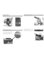
Dismantling of the Cassette Cover

1) Loosen 4 screws to remove the Cover Top (pos 255) of the

set.

2) Loosen 2 screws to remove the Panel Left (pos 253) and

2 screws to remove the Panel Right (pos 254) of the set.

3) Slide out the CDC Tray as shown in the diagram below with

the help of a flat head screw driver.

Cassette Cover

Remove Cassette Cover

Dismantling of the CDC Module and Front Panel

Remove CDC Module

4) Remove the Cover Tray CDC (pos 106) as indicated.

Front View CDC

Remove Cover Tray CDC

Dismantling of the CDC Module and Front Panel

Sliding Out The CDC Tray

5) Loosen 2 screws A and 2 screws B to remove the CDC

Module (pos 1105) as indicated.

6) Remove 2 screws (pos 226) at the bottom to separate the

Front Panel Assembly from the Plate Bottom (pos 265).

2

-1 

2

-1

3. Lift up and out

1. Place screw driver
    (flat side) between
    the cassette cover
    & cassette door

2. Twist screw driver

Summary of Contents for FWM15/21

Page 1: ...Tuner Board Systems Non Cenelec 7A ECO6 Tuner Board Systems Cenelec 7B ETF7 Tape Module 9 3CDC LC MP3CD2002 Module 10 Power 2001 Module 30 70W Version 11 AF9 Board 12 Set Mechanical Exploded view parts list 13 Revision List 14 Copyright 2004 Philips Consumer Electronics B V Eindhoven The Netherlands All rights reserved No part of this publication may be reproduced stored in a retrieval system or t...

Page 2: ...y FTD Clock Display x x ECO Standby Dark x x ECO6 Tuner board System Non Cenelec x x ECO6 Tuner board System Cenelec x x ETF7 Tape Module Non Autoreverse Ferro x x x x POWER 2001 Module 30 70W Version x x x x VERSION VARIATIONS Type Versions FWM390 Features Board in used ETF7 BOARD MAINS BOARD LEFT RIGHT AMPLIFIER SUPPLY BOARD MAINS SOCKET BOARD T U N E R B O A R D CD KEY BOARD FRONT BOARD KARAOKE...

Page 3: ...thin 3dB 50Hz 15kHz Dynamic Bass Boost DBB OFF DBB 1 DBB 2 DBB 3 2 Digital Sound Control Jazz Rock Techno Optimal 2 Headphone output at 32Ω 15mW 2dB 5mW 2dB CD mode Input sensitivity Aux CDR 500mV 1 0V at 600Ω CASSETTE RECORDER Number of track 2 x 2 stereo Tape speed 4 76 cm sec 2 Wow and flutter 0 4 DIN Fast wind rewind time C60 130 sec Bias system 75kHz 10kHz Rec Pb frequency response within 8dB...

Page 4: ...z e g 7122 707 48001 LF Voltmeter e g PM2534 DUT S N and distortion meter e g Sound Technology ST1700B Frame aerial e g 7122 707 89001 Tuner AM MW LW To avoid atmospheric interference all AM measurements have to be carried out in a Faraday s cage Use a bandpass filter or at least a high pass filter with 250Hz to eliminate hum 50Hz 100Hz RF Generator e g PM5326 Ri 50Ω Bandpass 250Hz 15kHz e g 7122 ...

Page 5: ...udio Burn in Test disc 1kHz 4822 397 30155 SBC429 Audio Signals disc 4822 397 30184 Dolby Pro logic Test Disc 4822 395 10216 ESD Equipment Anti static table mat large 1200x650x1 25mm 4822 466 10953 Anti static table mat small 600x650x1 25mm 4822 466 10958 Anti static wristband 4822 395 10223 Connector box 1MΩ 4822 320 11307 Extension cable to connect wristband to conn box 4822 320 11305 Connecting...

Page 6: ...n osservazione della più grande cauzione alla loro manipolazione Durante le riparazioni occorre quindi essere collegato allo stesso potenziale che quello della massa dell apparecchio tramite un braccialetto a resistenza Assicurarsi che i componenti e anche gli utensili con quali si lavora siano anche a questo potenziale Pour votre sécurité ces documents doivent être utilisés par des spécia listes ...

Page 7: ...ls right speaker to R and left speaker to L coloured marked wire to and black unmarked wire to 1 2 Fully inser t the stripped por tion of the speaker wire into the ter minal as shown Notes For optimal sound performance use the supplied speakers Do not connect more than one speaker to any one pair of speaker terminals Do not connect speakers with an impedance lower than the speakers supplied Please...

Page 8: ...ng for Demo on the system only to activate deactivate the demonstration for Clock on the system only to exit clock setting or cancel timer for Plug Play on the system only to exit plug play mode É Å PLAY PAUSE for CD MP3 CD to start or interrupt playback for Tape to start playback for Plug Play on the system only to initiate and start plug play mode í PREV ë NEXT TITLE for MP3 CD to select previou...

Page 9: ... a fuse this should have a value of 5 Amp If a plug without a fuse is used the fuse at the distribution board should not be greater than 5 Amp Note These vered plug must be disposed of to avoid a possible shock hazard should it be inserted into a 13 Amp socket else where How to connect a plug The wires in the mains lead are coloured with the following code blue neutral N brown live L As these colo...

Page 10: ...gnetising the heads Use a demagnetising tape available at your dealer RADIO RECEPTION Radio reception is poor If the signal is too weak adjust the antenna or connect an exter nal antenna f or better reception Increase the distance between the Mini HiFi System and your TV or VCR TAPE OPERATION RECORDING Recording or playback cannot be made Clean deck parts see Maintenance Use only NORMAL IEC I tape...

Page 11: ...ve Cassette Cover Dismantling of the CDC Module and Front Panel Remove CDC Module 4 Remove the Cover Tray CDC pos 106 as indicated Front View CDC Remove Cover Tray CDC Dismantling of the CDC Module and Front Panel Sliding Out The CDC Tray 5 Loosen 2 screws A and 2 screws B to remove the CDC Module pos 1105 as indicated 6 Remove 2 screws pos 226 at the bottom to separate the Front Panel Assembly fr...

Page 12: ...s 1101 A and 2 screws E as indicated to loosen the Karaoke Board pos 1101 D 1 The Knob Volume pos 139 can be remove by inserting a strong string into the slot and pull it out in the direction as indicated See picture 1 2 The Knob Rotary pos 138 can be remove by inserting a strong string into the slot and pull it out in the direction as indicated See picture 2 Picture 1 Picture 2 Repair Hints 1 Rem...

Page 13: ... 4 Due to the short flex cable wires in the ETF Module the pc board should be disconnected and reconnected on the reverse side of the tape mechanism to keep it electrically connected during repair See picture 3 Note The flex cables are very fragile care should be taken not to damage them during repair After repair be very sure that the flex cables are inserted properly into the flex sockets before...

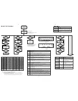
Page 14: ... and 10kHz for the Oversea 21 version the extended FM1 65 81MHz 74MHz is toggled on and off for East Eur 34 version Y N Y N Y N 2 Button pressed 2 Button pressed 9 Button pressed DISPLAY TEST Display shows Fig 2 and selected LEDs on see note 2 Display shows Fig 1 and selected LEDs on see note 1 Figure 1 Figure 2 note 2 Only DISC 2 TUNER AUX DSC VEC MAX SOUND are on note 1 All LEDs are on except EC...

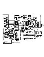
Page 15: ...F9 Rin 3k F AMPLIFIER 76dBA 16dB LEDS F2 CMOS 9V F2x TAPE CONTROL 5V6 HP DET MIC DET Vkk REG 5V6 9V POWER REG I2C DATA CONTROL 5V6_CON 5V6_CON A ATTN JOG 33R 5V6_CON REG 67dBA 1K 500mV REGISTER CDC CONTROL TUNER 28mV CD 5V 78dBA 3 2dB LED LOW_PWR_CTRL 5V 500mV HP DET 5V6 LED CLK NTC INCREDIBLE EEPROM F1x TMP87CS71F D DSC VEC DBB INTERFACE 3mV uP A CMOS IR EYE BASS 12A NOTE 125mV SIMPLE KARAOKE MIC...

Page 16: ...LEFT GND_A CD_RIGHT 5V_CD GND_M 1401 1 GND_A 7P 4P 1440 1531 1706 1 F 12A HP_DET 1701 12M TU_CLK 1 1 1402 11P 1 KEY2 220mm MIC_DET TU_DATA P04 KEY1 SH_DATA SILD 1500 FFC BD 1600 180mm FFC AD FFC SIDE FFC SIDE FFC TOP FFC TOP ETF7 180mm 120mm SW_INFO FFC SIDE GND_D 1104 TU_STEREO TU_CLK CD_RIGHT HP AUX IN 1501 1601 I2C_DATA I2C_CLK FFC AD 1503 1 TU_RIGHT FFC TOP FFC TOP 1701 1 LOW_PWR_CTRL ETF7 180...

Page 17: ...4 13G B1 B2 B3 B4 B5 B6 S5 B7 B8 B9 B10 B11 B12 11G B1 B2 B3 B4 B5 B6 S2 B7 B8 B9 B10 B11 B12 10G B1 B2 B3 B4 S1 B5 B6 B7 B8 S6 ALB MUTE TITLE DIM 1 2 3 NEWS AM LW FM MW m g n c p r e k j h f b col col Dp Dp d a B5 B4 B3 B2 B1 B5 B4 B3 B4 B6 B6 B6 B5 B4 B3 B2 B1 B6 B6 B7 B6 B5 B8 B11 B10 B9 B8 B7 B12 B12 B3 B2 B1 B2 B1 B11 B10 B9 B8 B7 14G 1G 8G 10G 13G 9G S7 S7 S1 S1 S2 S2 S3 S3 S4 S4 S5 S5 S6 S6...

Page 18: ...4x KEY1 KEY2 GND_D FE ST VK N 1 2 1440 3 4 1441 1442 A 3139 118 53880 88460 3442 pt 2a dd wk147 VARIATION TABLE Item No Features FWM390 30 FWM390 21 FWM390 22 25 RDS News x Simple Karaoke x Mic Detect x 1409 x x x 1424 1425 x 1427 x 1437 3486 1k 1k 1k 3511 10k 10k 3530 330R 3531 10k 10k 10k 3581 10k 10k 3595 3808 820R 4402 4404 6400 x x x 6403 x x x 6426 x 6440 x 6441 x x x 6447 x x x 6448 x x x 9...

Page 19: ...I2C_CLK 2485 100p 10K 3570 15p 22p 2457 74HC4094D 7405 D 1 2 3 4 MT1 5 MT2 TU 3465 1K 330R 3524 3516 10K 3458 100p 100n 2438 3594 560R FE ST VK N 1403 1 2 3 4 TU 3479 1K 6423 D 2454 2u2 1K 1432 1u 2423 470p 2439 47p 2452 10K 3508 100n 2410 6410 1N4148 D D 47p 2416 6439 1N4148 2474 10n TU 6447 1N4148 3534 M24C01 7403 3525 330R 470p 2442 3489 1K 4416 330R 3522 2 3 4 5 6 7 10p D 1u 2422 7410 BC847B 9...

Page 20: ...This assembly drawing shows a summary of all possible versions For components used in a specific version see schematic diagram and respective parts list 3139 113 3442 pt 2a dd wk147 FRONT PART COMPONENT LAYOUT ...

Page 21: ... 5 This assembly drawing shows a summary of all possible versions For components used in a specific version see schematic diagram and respective parts list 3139 113 3442 pt 2a dd wk147 FRONT PART CHIP LAYOUT ...

Page 22: ...is assembly drawing shows a summary of all possible versions For components used in a specific version see schematic diagram and respective parts list 3139 113 3442 pt 2a dd wk147 This assembly drawing shows a summary of all possible versions For components used in a specific version see schematic diagram and respective parts list 3139 113 3442 pt 2a dd wk147 This assembly drawing shows a summary ...

Page 23: ...D_A MIC 100n 2818 3800 GND_A 3K3 MIC 3811 100K 2804 2801 220n 3817 1n 2806 1M GND_A 1u 2817 5800 22u GND_A 20K 3807 RK09D 470n 2803 2805 470n 3806 33R MIC 3801 6K8 1801 FE BT VK N 1 2 3 4 10K 3814 3 4 5 6 4800 100n TC38 1800 9 8 7 1 2 1N4148 6800 1N4148 100n 2814 6801 GND_A MIC 3818 560R 1n 470R 3813 3803 4K7 7803 BC847B 2K7 3804 10K 3802 1n 2809 7805 BC847B BC847B 7802 3820 3K3 3816 DIPMATE 30 1 ...

Page 24: ...2785 47nF 50V 2480 4822 126 14305 100nF 10 16V 2481 4822 126 14305 100nF 10 16V 2484 4822 124 40769 4 7µF 20 100V 2485 4822 122 31765 100pF 2 63V 2486 4822 124 40248 10µF 20 63V 2487 4822 122 31765 100pF 2 63V 2600 4822 126 14494 22nF 10 25V 2602 4822 126 14494 22nF 10 25V 2603 4822 126 14305 100nF 10 16V 2800 4822 126 13193 4 7nF 10 63V 2801 4822 126 13879 220nF 80 20 16V 2802 3198 028 44790 47µF...

Page 25: ...062W 3807 2120 366 90291 Potm Rotary 20K 3808 4822 117 12968 820R 5 0 62W 3809 4822 051 30105 1M 5 0 062W 3810 4822 051 30331 330R 5 0 062W 3811 4822 117 13632 100k 1 0 062W 3812 4822 116 83883 470R 5 0 5W 4400 4822 051 30008 0R Jumper 0603 4401 4822 051 30008 0R Jumper 0603 4403 4822 051 30008 0R Jumper 0603 4416 4822 051 30008 0R Jumper 0603 4417 4822 051 30008 0R Jumper 0603 4420 4822 051 30008...

Page 26: ...57 62552 Coil 2 2µH 5 5800 4822 157 11235 Coil 22µH 5 DIODES 6400 4822 130 30621 1N4148 6401 4822 130 31878 1N4003G 6402 4822 130 30621 1N4148 6403 4822 130 31878 1N4003G 6404 4822 130 31878 1N4003G 6405 4822 130 34173 BZX79 B5V6 6406 4822 130 30621 1N4148 6409 4822 130 30621 1N4148 6410 4822 130 30621 1N4148 6411 9322 167 73676 LTL 4221NLC KA 6412 9322 161 99676 LTL 2R3VYKNT 6413 9322 161 99676 L...

Page 27: ... 6 5 43 C D 450kHz 450kHz 450kHz 20 75kHz VStabA VStabB VStabB VStabA VStabB 10 7 MHz 10 7 MHz 35 9 Vdd Vcc1 7 23 VStabA VStabB 38 34 22 Vcc2 8 ECO6 Systems 140499 LF filter RDS MPX RDS MPX stereo clock data enable Version 1120 1 8 FM Frontend AM Frontend AM FRAME AERIAL B 1103 1101 1102 A FM MPX buffer ampl 5 Discriminator 10 7 MHz Vdd Vcc1 Vcc Vcc2 AM RF AM Osc FM Osc FM RF FM IF 1 FM IF 2 AM IF...

Page 28: ...1n 3134 22K 6105 2 HN1V02H 100n 2163 T141 7KL 1K 3144 5102 3157 100K T109 470R 3153 2130 22n 220R 3105 3142 100K 3167 120R 33p 2149 2K2 3145 1132 C PAD T103 T111 2164 470n T102 2140 15p 2139 2138 2u2 82p 2133 1u 3103 8K2 T120 4p7 2154 3156 1101USA YKD21 100K 2161 100n 5119 2119 10p T142 5123 11p 2106 3172 6106 BAS216 100n 2165 5K6 3154 3155 220R 330R 2124 33K 3176 22n WRITE EN 5114 7P MUTE P0 P1 P...

Page 29: ...riginal frame antenna has to be used 2 RC network serves for damping the IF filter while adjusting the other one 4 MW has to be aligned before LW Waverange Input frequency Input Tuned to Adjust Output Scope Voltmeter FM 87 5 108MHz 65 81 74 87 5 108MHz FM MW version 9kHz grid 531 1602kHz as low as possible ECO6 System non Cenelec stage 3 120900 TUNER BOARD ECO6 Systems non Cenelec componentside vi...

Page 30: ...10 63V RDS only RESISTORS 3101 4822 051 20333 33kΩ 5 0 1W 3102 4822 117 10837 100kΩ 1 0 1W 3103 4822 051 20822 8 2kΩ 5 0 1W 3104 4822 117 13577 330Ω 1 0 1W 3105 4822 117 11503 220Ω 5 0 1W 3132 4822 051 20479 47Ω 5 0 1W 3134 4822 051 20223 22kΩ 5 0 1W 3141 4822 117 11148 56kΩ 1 0 1W 3142 4822 100 12159 TRIMPOT 100kΩ RESISTORS 3143 4822 051 20223 22kΩ 5 0 1W RDS only 3144 4822 051 10102 1kΩ 2 0 25W ...

Page 31: ... B V Stab B V Stab A V Stab B 10 7 MHz 10 7 MHz 35 9 Vdd Vcc1 7 23 V Stab A V Stab B 38 34 22 Vcc2 8 ECO6 Systems Cenelec 140499 V Loop FM AM RF AM Osc FM IF 1 FM IF 2 LF filter MPX buffer ampl RDS MPX 5 RDS MPX stereo clock data enable Version 3 1120 AM IF 1 AM IF 2 AM AFC 1 8 AM Frontend 2 AM FRAME AERIAL B 1103 1101 1102 A FM AM FM Discriminator 10 7 MHz Vdd FM Vcc1 Vcc Vcc2 MW LW AM RF AM Osc ...

Page 32: ...4 22n USA 22n USA C PAD 1131 T141 2106 11p 20p_LW 0R 4104 0R 41xx 2165 100n 1130 C PAD 10K 3180 2150 100n BZX284 C11 6107 T102 2127 220n 2169 2n2 100K 3170 1 I 3 O 2125 560p 5109 2 G 470R 3152 2108 100p 3125 10K 3153 470R 330R 3193 T103 120R 3167 100R 3195 7 8 33K 3176 8 5122 1 2 3 4 6 5123 1 2 3 4 6 7 5110 G 2 I 1 O 3 5115 1 2 3 4 6 7 8 2 3 4 6 7 8 5119 1 2135 100n 2163 LW 7104 BC337 40 2145 220p...

Page 33: ...ce Testprogram By selecting the TUNER TEST test frequencies will be stored as preset frequencies automatically AM FRAME AERIAL FM 75Ω FM FRONTEND Birdy Filter ECO6 Sys Cenelec layout stage 8 200803 1101 B5 1102 B5 1103 C5 1110 B4 1120 A4 1130 A5 1131 C5 1132 A4 2106 B4 2107 B3 2128 A3 2129 B3 2133 C1 2138 B1 2144 B1 2162 A4 2191 B4 3142 C2 5102 C4 5103 C4 5109 B3 5110 A2 5111 A3 5112 A2 5114 A2 51...

Page 34: ...6W 3131 3198 021 38210 820Ω 5 0 06W 3132 4822 051 20479 47Ω 5 0 1W 3134 4822 051 20223 22kΩ 5 0 1W 3135 3198 021 31020 1kΩ 5 0 06W 3137 4822 051 20223 22kΩ 5 0 1W LW only 3141 4822 117 11148 56kΩ 1 0 1W 3142 4822 100 12159 TRIMPOT 100kΩ 3143 4822 051 20223 22kΩ 5 0 1W RDS only 3144 4822 051 10102 1kΩ 2 0 25W RDS only 3145 4822 117 11449 2 2kΩ 1 0 1W 3146 4822 051 20229 22Ω 5 0 1W 3150 4822 117 108...

Page 35: ...ouble deck H L CRO2 Mechanism B Mechanism A Not for Ferro version Chrome Ferro Chrome Ferro Ferro 2624 100nF 2701 2702 150pF 270pF 270pF 2703 2704 100pF 220pF 220pF 2717 2718 10nF 15nF 15nF 2721 2722 6 8nF 6 8nF 2727 2728 470pF 1nF 1nF 3616 10k 1k 1k 3618 6k8 3620 10k trimmer 3622 10k trimmer 10k trimmer 3672 4k7 3676 47k 3687 220R 220R 3688 680R 3723 3724 15k 18k 18k 3725 3726 10R 10R 3727 3728 5...

Page 36: ...952BT 1A0 1A1 1A2 Rec current ATTEN ALC PLAYBACK EQUALISATION PB EON SW HEF4952BT 2A0 2A1 2A2 MPX 1A0 1A1 PB A ADJ PB B ADJ Rec In PB In 2A2 DOLBY B NR CXA1101M REC Out PB Out REC ADJ SHIFT REGISTER HEF4094BT 3A0 3A1 3A2 HS REC CRB DOLBY NOM HI SPEED REC EON 3A0 NS 2A2 MUTE For Dolby version only PB Out ATTEN 4794 9792 CLK DATA STROBE For Non dolby version only Only 1 channel is presented NOTE Mic...

Page 37: ...iable resistor 3773 for adjusting the optimal level of the bias current for Ferro or Chrome 11 Bias Symm For Dolby B NR version only Bias Symm making use of the Variable resistor 3785 to adjust the bias current for the left and the right channel to be equal 12 PB Switch Playback Switch which consists of the FETs 7785 For Dolby B NR version only 7786 J111 is for the purpose of providing a virtual g...

Page 38: ... for motor 13 CrO2 A Chrome tape detection switch deck A open Cr close Fe 14 H H pin for motor CONNECTORS ASSIGNMENTS CONNECTOR 1701 INTERCONNECTION TO AF BOARD 1 REC L Record input left 2 REC R Record input right 3 GND A AF Ground 4 TAPE L Playback output left 5 12V D C supply 12V for AF electronics 6 TAPE R Playback output right 7 CMOS Negative d c supply 9V for CMOS ICs CONNECTOR 1703 INTERCONN...

Page 39: ...ure 1 f Hz level dB 8dB 6dB 12 5k 4k 250 80 8dB f Hz level dB 8dB 10dB HSD 6dB 10k 4k 250 100 8dB 10dB HSD figure 2 check SBC419A 4822 397 30069 SBC420 4822 397 30071 SBC420 3150Hz SBC420 10kHz SBC420 DECK A B SBC419A SBC420 SBC419A or SBC420 SBC419A or SBC420 1 B Rec Switch REV Rec R CrO2 CrO2 Rec F Solenoid B Mode A Mode Solenoid Motor R1 680R R2 680R A Photo Sensor B Photo Sensor 2 B CrO2 Switc...

Page 40: ...LAYOUT CHIP LAYOUT 3139 113 3409 pt2 dd wk0042 3 4 2 1 6 5 3139 113 3409 pt2 dd wk0042 Some location on this board is prepared for both 0603 0805 SMDs footprint in such locations 0603 SMDs may be substituted 3 4 2 1 6 5 ...

Page 41: ...QUALISATION 1 1 REC R S4 PLAYBACK 0 1 S1 ANALOG CCTRY 1 1 0 S2 S1 S3 AN7323S 0 1 1 BIAS 4n7 2726 7784 BC857B 1M 3787 100n 2746 A0 7 A1 9 A2 10 VDD HEF4952B 7730 7782 220R 3701 C B4 A 3789 47K A A 2784 15n 1N4148 6778 7792 BC847B P 2706 220p 2A0 33n 2719 3736 22K 3760 120R A A 1N4148 6776 P 3K3 7786 J111 470p 2727 3K9 3722 2742 1K2 1M 3780 47u 2763 100p 2711 100n 2741 15K 3723 3703 220R 6K8 3769 37...

Page 42: ...10K mode_B Vcc CrO2_B 10K 47K 3676 7618 BC847B 100n 2626 M 5 1A0 1703 1 1N4003 6611 100n 2624 100K 3628 3679 47K 120K 3610 PMBT2907 7613 CRB 100K 3685 P 7610 HEF4094BT M 100K 3686 2A1 3601 2K2 680R 3688 3608 MOTOR M L CLK L 1 VDD 16 8 VSS CP 3 D 2 E0 15 4 O0 5 O1 O2 6 7 O3 14 O4 13 O5 12 O6 11 O7 Os 9 Os 10 STR MOTOR 56K 3612 7619 BC847B 5 6K8 3618 1702 3604 56K 5 3623 100K CRA 3613 27K 3622 BC857...

Page 43: ...normal service spare parts TAPE MODULE EXPLODED VIEW 1 3139 118 77130 Autoreverse Mech CWE44FR01 1 3139 118 77140 Non Autoreverse Mech CWE44FF02 Chrome Ferro 1 3139 118 77950 Non Autoreverse Mech CWE44FF05 Ferro 3 Screw D3 x 10 6 Screw M2 x 16 7 3139 110 34080 Flex Cable 14 pin 7 5 cm Note Only the parts mentioned in this list are normal service spare parts ...

Page 44: ... Arm Assembly R 23 9965 000 02314 Coil Assembly 25 9965 000 06443 Cam Gear 32 4822 528 11209 Flywheel Assembly RV 42 9965 000 02315 Belt AF Autoreverse deck 42 9965 000 02718 Belt AF Non autoreverse deck 69 4822 492 11761 Spring 102 4822 532 12931 Washer 103 4822 532 12932 Washer 104 4822 532 12933 Washer Note Only the parts mentioned in the list are normal service spare parts ...

Page 45: ...00 06443 Cam Gear 32 4822 528 11209 Flywheel Assembly RV 44 2 9965 000 02317 Flex Socket 14 Pin 44 3 9965 000 02320 Photo Interrupter 44 4 4822 050 16801 680R 1 0 4W 44 6 9965 000 02318 Leaf Switch 44 7 9965 000 02319 Mode Switch 59 9965 000 02719 Belt BF Large 69 4822 492 11761 Spring 102 4822 532 12931 Washer 103 4822 532 12932 Washer 104 4822 532 12933 Washer Note Only the parts mentioned in th...

Page 46: ...02320 Photo Interrupter 44 4 4822 050 16801 680R 1 0 4W 44 6 9965 000 02318 Leaf Switch 44 7 9965 000 02319 Mode Switch 45 9965 000 02323 Rec Pb Head Assembly 50 4822 402 10973 Pinch Arm Assembly L 54 9965 000 02324 Flywheel Assembly L 69 4822 492 11761 Spring 73 4822 492 11762 Spring 101 9965 000 02325 Washer 102 4822 532 12931 Washer 103 4822 532 12932 Washer 104 4822 532 12933 Washer 107 9965 0...

Page 47: ...se 3678 482211710834 47k 1 0 1W 3679 482211710834 47k 1 0 1W 3680 482211710834 47k 1 0 1W 3685 482211652234 100k 5 0 5W 3686 482211710837 100k 1 0 1W 3687 482211711503 220R 1 0 1W not for Ferro 3688 482211710361 680R 1 0 1W Autoreverse 3701 482211711503 220R 1 0 1W 3702 482211711503 220R 1 0 1W 3703 482211711503 220R 1 0 1W 3704 482211711503 220R 1 0 1W 3705 482211711503 220R 1 0 1W 3706 482211711...

Page 48: ... Jumper 0805 4745 482205120008 0R Jumper 0805 4746 482205120008 0R Jumper 0805 4748 482205120008 0R Jumper 0805 4785 482205120008 0R Jumper 0805 only for Ferro 4790 482205120008 0R Jumper 0805 4794 482205120008 0R Jumper 0805 4795 482205120008 0R Jumper 0805 COILS FILTERS 5701 482215711477 Coil 2 2µH 5 5703 482215620946 Osc Coil 100kHz DIODES 6611 482213031878 1N4003G 6612 482213031878 1N4003G 661...

Page 49: ...ram 10 4 Blockdiagram 10 5 CD PART Component Layout Main Board 10 6 Circuit Diagram 10 7 MP3 PART Component Layout Main Board 10 8 Circuit Diagram 10 9 Exploded View 10 10 Partslist 10 12 3CDC LC MP3CD2002 3 Disc Carousel Changer MP3 Board Layout stage 2 ...

Page 50: ... WHEN CONNECTING A NEW CD MECHANISM THAT S WHY BESIDES THE SAFETY MEASURES LIKE SWITCH OFF POWER SUPPLY ESD PROTECTION ADDITIONAL ACTIONS MUST BE TAKEN BY THE REPAIR TECHNICIAN fig 1 Attention The laser diode of this CD drive is protected against ESD by a solder joint which shortcircuits the laserdiode to ground For proper functionality of the CD drive this solder joint must be removed after conne...

Page 51: ... of Tray Service hints 1 Open the tray 2 Release 2x catch as shown in fig 2 and Detail A 3 Pull tray out fig 2 Assembling of Tray 1 Turn Cam pos 48 clockwise to end position 2 If necessary move Guiding pos 49 to the right end position 3 Insert the Tray ...

Page 52: ...10 4 Wiring Disc Motor Inner switch Slide Motor Service Position ...

Page 53: ... endposition Open during movement Open if the drive is in one endposition Closed during movement VDD pin 16 EN1 pin 15 Power on FOCUS MOTOR RADIAL MOTOR SLEDGE MOTOR MOTOR TURNTABLE 7803 7802 TDA7073A TDA7073A TTM TTM SLEDGE SLEDGE RAD RAD FOC FOC 55 54 56 59 60 M1 M2 SL RA FO MP3 Version 1802 5 3 7 4 10 11 12 1805 1805 9 7 SHR DATA 6 12 13 10 11 9 CD_IIS_DATA IIS_WCLK IIS_SCLK External MP3 Decode...

Page 54: ...3 3825 E3 3826 E3 3827 D4 3828 D2 3829 F3 3830 F4 3832 C3 3833 E4 3834 E4 3836 E2 3837 D2 3838 D2 3839 E3 3840 C3 3842 D2 3843 E2 3844 F1 3845 D2 3846 E2 3847 E2 3848 D3 3849 C3 3850 D1 3853 E4 3854 E3 3855 E3 3856 F4 3857 F4 3858 C2 3859 C2 3860 C2 3861 C2 3862 C4 3863 D2 3864 E4 3865 C4 3866 F3 3867 E4 3871 E2 3872 E3 3878 C3 3881 C3 3882 E2 3883 E2 3884 E3 3885 E2 3890 F4 3891 E2 4700 B2 4701 B...

Page 55: ...4 13 12 11 9 10 1881 6803 BAS216 4x 6808 1882 1883 3776 10K 3771 220p 2883 2877 82p 1K 470R 3772 10K 3773 10K 3766 1K 220p 2878 10K 3765 33K 3730 3770 15 1 16 1875 1876 3 5 3 1 1875 1876 1 5 SW_INFO Power on Output enable delay BC847B 7812 2872 47n BZX284 C5V1 6805 4u7 2881 BAS216 6804 3715 100K 3755 220R 22K 3713 10K 3714 220R 3754 10V TRAY MOTOR CAROUSEL MOTOR Changer Control Logic Internal Supp...

Page 56: ...50 B4 7452 C2 7453 C2 7454 C3 7455 D2 7457 B4 7460 B2 1451 B5 1455 A4 2450 C1 2451 B1 2452 C2 2453 B1 2454 B1 2455 D2 2457 A2 2461 D4 2463 A3 2464 D4 2465 D4 2466 A3 2467 B4 2468 B4 2469 B4 2472 D3 3450 C1 3451 B1 3454 D2 3465 C1 3467 A3 3468 A3 3469 C4 3470 D3 3471 C4 3473 C4 3474 A3 3475 C4 3476 C4 3477 B4 3479 A2 3480 C4 3481 C4 3484 B4 3490 A4 3494 A2 3496 A4 3499 C1 4450 A4 6451 D4 7451 B3 74...

Page 57: ...BDX2 60 BFSR0 43 36 BFSR1 44 BFSR2 BFSX0 53 73 BFSX1 BFSX2 54 31 BIO 77 CLKMD1 78 CLKMD2 79 CLKMD3 CLKOUT 94 CVDD1 12 A3 134 A4 136 A5 137 A6 138 A7 139 A8 140 A9 141 BCLKR0 41 BCLKR1 38 BCLKR2 42 BCLKX0 48 71 BCLKX1 BCLKX2 49 BDR0 45 35 BDR1 BDR2 47 A1 132 A10 5 A11 7 A12 8 A13 9 A14 10 A15 11 A16 105 A17 107 A18 108 109 A19 A2 133 110 A20 A21 143 A22 2 7451 A0 131 2466 100n 2463 3474 15R 1u 3465...

Page 58: ...6560 SUPPORT 31 4822 529 10386 RUBBER DAMPER CD DRIVE REAR 32 4822 529 10387 RUBBER DAMPER CD DRIVE FRONT 33 3103 304 06970 WASHER 35 3103 309 05350 CD DRIVE MCD1B 41 3103 304 66480 FRAME 42 3103 304 66540 BRACKET GUIDING 43 3103 301 06460 SPRING GUIDING 44 3103 304 06890 GEAR 3 45 3103 304 06980 NAIL FIXATION 46 3103 304 06880 GEAR 2 47 3103 304 66530 BRACKET LOAD 48 3103 304 06910 CAM 49 3103 30...

Page 59: ...WER BLACK 21 3103 304 66490 CAROUSEL BLACK 22 3103 304 06860 PULLEY DRAWER 23 3103 304 06850 ECCENTRIC GEAR WHEEL 24 3103 304 06980 NAIL FIXATION 25 3103 304 66850 DRIVING BELT CAROUSEL 27 4822 532 12365 BUSH DRAWER height 5 5mm d 9 4mm 29 3103 304 66550 BRACKET DISC 30 3103 304 66520 TUMBLER 31 3103 301 06470 SPRING DISC 32 3103 304 06920 CONTROL DISC 34 3103 304 06870 GEAR 1 37 4822 361 10753 CA...

Page 60: ...2 126 13883 220pF 5 50V 2865 5322 122 32654 22nF 10 63V 2866 4822 126 13751 47nF 10 50V CAPACITORS 2867 4822 126 13883 220pF 5 50V 2868 2020 552 94427 100pF 5 50V 2869 2020 552 94427 100pF 5 50V 2872 3198 024 44730 47nF 5 50V 2873 4822 124 80231 47µF 20 16V 2876 4822 124 12245 220µF 20 16V 2877 4822 126 14226 82pF 50V 2878 4822 126 13883 220pF 5 50V 2879 4822 124 12245 220µF 20 16V 2880 4822 124 1...

Page 61: ...MPER 0805 4708 4822 051 20008 CHIP JUMPER 0805 4709 4822 051 20008 CHIP JUMPER 0805 4710 4822 051 20008 CHIP JUMPER 0805 4711 4822 051 20008 CHIP JUMPER 0805 4712 4822 051 20008 CHIP JUMPER 0805 4713 4822 051 20008 CHIP JUMPER 0805 4714 4822 051 20008 CHIP JUMPER 0805 4715 4822 051 20008 CHIP JUMPER 0805 4716 4822 051 20008 CHIP JUMPER 0805 4717 4822 051 30008 CHIP JUMPER 0603 4718 4822 051 20008 ...

Page 62: ... 4822 051 20008 CHIP JUMPER 0805 4886 4822 051 20008 CHIP JUMPER 0805 4887 4822 051 30008 CHIP JUMPER 0603 4888 4822 051 20008 CHIP JUMPER 0805 4889 4822 051 20008 CHIP JUMPER 0805 4890 4822 051 20008 CHIP JUMPER 0805 4891 4822 051 30008 CHIP JUMPER 0603 RESISTORS 4892 4822 051 20008 CHIP JUMPER 0805 4893 4822 051 20008 CHIP JUMPER 0805 4894 4822 051 20008 CHIP JUMPER 0805 4895 4822 051 20008 CHIP...

Page 63: ...03 10kΩ 5 0 06W 3468 4822 051 30103 10kΩ 5 0 06W 3469 4822 051 30101 100Ω 5 0 06W 3470 4822 117 12971 15Ω 5 0 06W 3471 4822 051 30339 33Ω 5 0 06W 3472 4822 051 30154 150kΩ 5 0 06W 3473 4822 117 13632 100kΩ 1 0 06W RESISTORS 3474 4822 117 12971 15Ω 5 0 06W 3475 4822 051 30101 100Ω 5 0 06W 3476 4822 051 30101 100Ω 5 0 06W 3477 4822 051 30471 470Ω 5 0 06W 3478 4822 051 30471 470Ω 5 0 06W 3479 4822 05...

Page 64: ...erate as so called super class G amplifiers The supply pins 12 Vcc are not just connected to one fixed DC supply as in conventional amplifiers Dependent on the output power there are three different DC voltages supplied to the power amplifiers C1 20V for low output power B1 29V for medium output power A1 41V for high output power Principle benefit of Super Class G Conventional power stage Class G ...

Page 65: ...ration of A1 Common full wave rectifying with bridge rectifier 6202 using 100 secondary winding of mains transformer pin 10 14 Generation of B1 The supply for B1 consists of one full wave rectifier 2 diodes of bridge rectifier 6202 with 6200 6220 in parallel 6201 6221 in parallel for generation of B1using approx 70 secondary winding of mains transformer pin 10 13 respectively pin 11 14 As example ...

Page 66: ...used for monitoring the transformer temparature LOW_PWR_SUP is used to supply the microprocessor during ECO stand by is used for filament of display Vkk supply of display supply for Power amplifier Super Class G LEFT RIGHT from Source Selector on Audio Frequency Board 6210 6214 5203 Stand by Transformer B1 LOW_PWR_CNTRL C1 5V6 5V_VCD VCD_ON 7330 VCD_ON Blockdiagram Power2001 30 70W 26 09 2000 12V ...

Page 67: ...2 C5 6213 B5 6214 B5 6215 D5 6216 C5 6217 C5 6218 C5 6220 B3 6221 B3 6222 B5 7200 A2 7201 D5 7202 C5 7203 A3 9206 B2 9208 B1 9210 D1 9211 D4 9212 D5 9213 D4 9214 C5 9216 B4 9217 B3 9218 C4 9219 C1 9220 C3 9221 D3 9222 D3 9223 C4 9224 B4 9225 B4 9226 D4 9227 B4 9228 D3 9229 C5 9230 C3 9231 D3 9232 D2 9233 D3 9234 D2 9235 C3 9236 C3 9237 C3 9238 C3 9239 C3 9240 C2 9241 C2 9242 B5 9243 A4 9244 A5 924...

Page 68: ... 4K7 3205 5203 1 10 5 6 8 BZX79 C33 6207 6201 1N5392 1N5392 6220 6221 1N5392 T5A 1200 19372 1N4003 6214 4m7 2217 C1 9214 3211 4R7 5202 97TS 6 7 8 9 11 12 13 14 15 16 17 2 3 4 5 5001 1 10 6m8 2216 6206 1N4003 T1 6A 1208 4K7 3208 3207 4K7 NTC F1 ECO F2 NTC LOW_PWR_SUP LOW_PWR_SUP LOW_PWR_SUP ECO F2 F1 not on all versions not on all versions Mains Transformer Voltage Selector Stand by Transformer Sta...

Page 69: ...11 6 POWER BOARD COPPERSIDE VIEW P2001 30 70W AN17850 PWR313 11 6 ...

Page 70: ... F300 A1 F301 A1 F302 A1 F303 A1 F304 A1 F305 A4 F306 B9 F307 B13 F308 B2 F309 C1 F310 D13 F311 C3 11 6V CDR ONLY 5V T1A 24 2V _CNTRL 41V 40V TO SUPPLY MAINS 0 6V 7 5V F312 C1 F313 C9 F314 C1 F315 D1 F316 D1 F317 D1 F318 D13 F319 E3 F320 D2 F322 E2 F324 E2 F325 E11 F326 E11 F327 E2 F328 F11 F329 F2 F330 E9 F331 F11 F332 G1 F333 G1 F334 G1 _SUPPLY LOW_PWR A1 CDR ONLY 10K 3336 BC557B 7303 6313 1N414...

Page 71: ... 3333 4822 116 52199 68Ω 5 0 16W 3336 4822 050 21003 10kΩ 2 0 25W 3337 4822 116 52206 120Ω 5 0 5W 3338 4822 116 52176 10Ω 5 0 5W 3339 4822 116 52269 3 3kΩ 5 0 5W 3340 4822 116 83872 220Ω 5 0 5W 3341 4822 116 52283 4 7kΩ 5 0 5W RESISTORS 3343 4822 116 52285 470kΩ 5 0 5W 3344 4822 050 21003 10kΩ 2 0 25W 3345 4822 116 83876 270Ω 5 0 16W 3346 4822 116 52249 1 8kΩ 5 0 16W 3347 4822 116 52249 1 8kΩ 5 0 ...

Page 72: ...IBLE SURROUND IS The AF9 provides 2 possible IS namely a Simple IS using TDA7468D with addition of passive network b Full IS using transistor circuitry to create phase shifting and spatial effect g HEADPHONE AMPLIFIER Headphone amplifier NJM4556AM 7601 is provided after the Sound processor 7501 to drive 32 ohm to 1kohm headphone h M62320FP The M62320FP 7403 I2 C Expander provides additional contro...

Page 73: ...CHIP LAYOUT 12 2 12 2 This assembly drawing shows a summary of all possible versions For components used in a specific version see schematic diagram and respective parts list 3139 113 3435 pt4 dd wk0142 ...

Page 74: ...3 12 3 COMPONENT LAYOUT This assembly drawing shows a summary of all possible versions For components used in a specific version see schematic diagram and respective parts list 3139 113 3435 pt4 dd wk0142 ...

Page 75: ...12 4 12 4 SOURCE SELECTION SOUND PROCESSING CIRCUIT ...

Page 76: ...12 5 12 5 HEADPHONE AMPLIFIER I2 C EXPANDER CIRCUIT 1K ...

Page 77: ...GND_D T101 1520 FE BT VK N 1 2 3 4 aa 5V6_Con 4905 9405 T094 DPL_L GND_EMC T110 T059 T108 T060 D_Text 12V_M 4904 I2C_Clk CD_Right T085 GND_D T078 470p 2950 2952 100p 47p 2810 3205 5K6 T090 T119 DSA_STB 470p 2951 T066 GND_D T086 D_Text MIC_DET 4906 T053 T084 T072 14 2 3 4 5 6 7 8 9 aa 1205 1 10 11 12 13 5V6_Con GND_D F1 DPL_Clk AMP_RIGHT T069 EH B 1524 1 2 3 14 15 2 3 4 5 6 7 8 9 1100 1523 FE BT VK...

Page 78: ...06 2238 916 15641 22nF 10 X7R 25V 2603 4822 124 81151 22µF 50V 2207 4822 124 40433 47µF 20 25V 2604 4822 124 81151 22µF 50V 2208 4822 126 13879 220nF 80 20 16V 2605 2020 552 94427 100pF 5 NP0 50V 2209 4822 124 41751 47µF 20 50V 2606 2020 552 94427 100pF 5 NP0 50V 2210 4822 126 13879 220nF 80 20 16V 2607 4822 126 13881 470pF 5 50V 2401 2020 552 94427 100pF 5 NP0 50V 2608 4822 126 13881 470pF 5 50V ...

Page 79: ...Ω 5 0 062W 3550 4822 051 30183 18K 5 0 062W 3689 4822 051 30151 150Ω 5 0 062W 3591 5322 117 13056 8 2K 1 0 063W 3692 4822 051 30334 330K 5 0 062W 3592 5322 117 13056 8K2 1 0 063W 3694 4822 051 30222 2 2K 5 0 062W 3593 4822 051 30562 5 6K 5 0 063W 3707 4822 051 30102 1K 5 0 062W 3594 4822 051 30562 5 6K 5 0 063W 3708 4822 051 30102 1K 5 0 062W 3601 4822 116 52238 12K 5 0 5W 3711 4822 051 30562 5 6K...
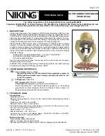
Page 80: ...13 1 13 1 EXPLODED VIEW MAIN UNIT ...

Page 81: ... 19P AD 132 3140 117 69801 BUTTON SET SOURCE 1403 3139 110 34610 FFC FOIL 11P 180 11P AD 134 3140 117 71031 BTN SET C PROG N VCD 1500 3139 110 33960 FFC FOIL 04P 120 04P BD 135 3140 117 69811 BUTTON MAX 1501 3139 110 33960 FFC FOIL 04P 120 04P BD 21 136 3140 117 69822 BUTTON DSC DBB VEC IS 1600 3139 110 35050 FFC FOIL 08P 220 08P AD 137 3140 117 71071 RING VOLUME 1700 4822 320 12752 7P 180MM 138 3...

Page 82: ...REVISION LIST 14 1 1 1 Manual3140 785 32811 Chapter 11 the power board and the parts list of the Power 2001 Module have been updated Refer to page 11 6 to 11 8 ...

Reviews: