background image

1-2

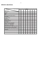
VERSION VARIATIONS

/55

Karaoke

News

RDS

Rotary Encoder (volume control)

x

Jog Shuttle

Voltage Selector

Aux Input

x

Digital Output

Headphone Socket

x

Line Output

Matrix Surround Loudspeakers

Standby - FTD Clock Display

ECO Standby - LED Display

x

ECO6 Tuner board - System Non-Cenelec

x

ECO6 Tuner board - System Cenelec

ETF7 Tape Module: Non-Autoreverse Ferro

Type /Versions:

FWM58

3

Features &
Board in used:

USB Direct

x

x

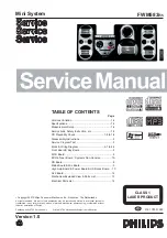
Summary of Contents for FWM583

Page 1: ...n The Netherlands Subject to modification GB 3141 785 31980 Mini System TABLE OF CONTENTS Page Versions Variation 1 2 Specifications 1 3 Measurement Setup 1 4 Service Aids Safety Instruction etc 1 5 CD Playability Check 1 6 to 1 8 Disassembly Instructions 2 Service Program Test 3 Block Wiring Diagram 4 1 to 4 2 Front Board Key Board 5 MCU Board 6 ECO6 Tuner Board Systems Non Cenelec 7A CD Board 8 ...

Page 2: ...Aux Input x Digital Output Headphone Socket x Line Output Matrix Surround Loudspeakers Standby FTD Clock Display ECO Standby LED Display x ECO6 Tuner board System Non Cenelec x ECO6 Tuner board System Cenelec ETF7 Tape Module Non Autoreverse Ferro Type Versions FWM583 Features Board in used USB Direct x x ...

Page 3: ...dvised Sampling frequencies 32 44 1 48 kHz TUNER FM wave range 87 5 108 MHz MW wave range 9 kHz 531 1602 kHz MW wave range 10 kHz 530 1700 kHz Tuning grid 9 10 kHz Number of presets 40 Antenna FM 75 wire MW Loop antenna USB PLAYER USB 12 Mb s V1 1 support MP3 and WMA files Number of albums folders maximum 99 Number of tracks titles maximum 400 SPEAKERS System 2 way double port bass reflex Impedanc...

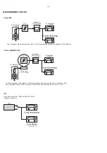
Page 4: ...122 707 89001 Tuner AM MW LW To avoid atmospheric interference all AM measurements have to be carried out in a Faraday s cage Use a bandpass filter or at least a high pass filter with 250Hz to eliminate hum 50Hz 100Hz RF Generator e g PM5326 Ri 50Ω Bandpass 250Hz 15kHz e g 7122 707 48001 LF Voltmeter e g PM2534 DUT RF Generator e g PM5326 S N and distortion meter e g Sound Technology ST1700B Use a...

Page 5: ...ICE AIDS GB WARNING All ICs and many other semi conductors are susceptible to electrostatic discharges ESD Careless handling during repair can reduce life drastically When repairing make sure that you are connected with the same potential as the mass of the set via a wrist wrap with resistance Keep components and tools also at this potential ESD CLASS 1 LASER PRODUCT GB Safety regulations require ...

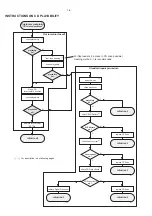
Page 6: ...ce CD Drive Laser current ok N Y check Laser current CD Drive offsets ok N Y check CD Drive offsets clean the lens check playability return set Customer complaint CD related problem return set return set replace CD Drive return set replace CD Drive return set replace Signal Processor return set fast lens cleaning 1 2 3 4 5 6 7 For flap loaders access to CD drive possible cleaning method 4 is recom...

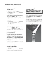
Page 7: ...o contact the workshop directly The lens cleaning method 3 should be mentioned in the addendum sheet The final wording in national language as well as the printing is under responsibility of the Regional Service Organizations 3 FAST LENS CLEANING dry brush Use lens cleaning CD SBC AC300 9082 100 00043 Insert the lens cleaning CD press PLAY and follow the voice guide s instructions on the CD 4 LIQU...

Page 8: ... a DC Millivoltmeter directly on the connector see drawing below Pin numbering varies from drive to drive The values from diode A D should read 0 10mV Diodes E and F are less critical If one of the offsets is higher than 10mV the CD drive has to be replaced Otherwise replace the Signal Processor Sanyo DA12T3 CD Drive A A F C B E C D E VCC B VREF F D 9 10 11 12 13 14 15 16 1800 5V_HF VrefCD10 A D E...

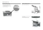
Page 9: ...am below with the help of a flat head screw driver Dismantling of the CDC Module and Front Panel Remove CDC Module 4 Remove the Cover Tray CDC as indicated Front View CDC Remove Cover Tray CDC Dismantling of the CDC Module and Front Panel Sliding Out The CDC Tray 5 Loosen 2 screws A and 2 screws B to remove the CDC Module as indicated 6 Remove 2 screws at the bottom to separate the Front Panel Ass...

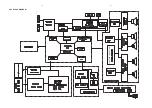
Page 10: ...74HCT04D HEF4013BT 4 1 4 1 SET BLOCK DIAGRAM ...

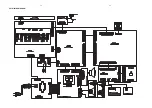
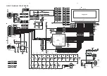
Page 11: ...4 2 4 2 SET WIRING DIAGRAM ...

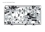
Page 12: ...5 1 5 1 PCB LAYOUT FRONT BOARD TOP VIEW ...

Page 13: ...5 2 5 2 PCB LAYOUT FRONT BOARD BOTTOM VIEW ...

Page 14: ...239 1K5 R239 1K5 TP222 TP222 R251 5K6 R251 5K6 TP221 TP221 TP236 TP236 TP229 TP229 C244 470pF C244 470pF C206 47uF C206 47uF C248 470pF C248 470pF TP216 TP216 C201 47uF C201 47uF C250 470pF C250 470pF R211 2K2 R211 2K2 R203 1K R203 1K SW220 TITLE SW220 TITLE TP230 TP230 TP1 TP1 C242 470pF C242 470pF J201 Phone Jack J201 Phone Jack 3 4 5 6 7 8 9 TP235 TP235 SW224 DBB SW224 DBB R232 10K R232 10K C23...

Page 15: ...W205 DISC3 SW205 DISC3 SW203 DISC1 SW203 DISC1 R249 120K R249 120K SW201 OPEN CLOSE SW201 OPEN CLOSE SW204 DISC2 SW204 DISC2 R244 5K6 R244 5K6 SW202 DS_CHANGE SW202 DS_CHANGE TP203 TP203 TP202 TP202 TP200 TP200 CN204 CON_4PIN_FFC_1 27mm CN204 CON_4PIN_FFC_1 27mm P1 1 P2 2 P3 3 P4 4 TP201 TP201 CIRCUIT DIAGRAM KEY BOARD ...

Page 16: ...6 1 6 1 PCB LAYOUT MCU BOARD TOP VIEW ...

Page 17: ...6 2 6 2 PCB LAYOUT MCU BOARD BOTTOM VIEW ...

Page 18: ...IO_A 9 SCL BW 115 GPIO_A 10 SDA 116 GPIO_A 11 SCL 117 USBH 0 _D GPIO_B 29 79 USBH 0 _D GPIO_B 28 80 USBH 1 _D GPIO_B 27 82 USBH 1 _D GPIO_B 26 83 UART 0 _TXD GPIO_B 8 62 UART 0 _RXD GPIO_B 9 63 BM 0 GPIO_B 21 BCLK 86 BM 1 GPIO_B 22 LRCK 87 GPIO_B 23 MCLK 88 BM 2 GPIO_B 24 DAO 89 GPIO_B 25 DAI 90 XIN 55 XOUT 54 XFILT 75 XTIN 57 XTOUT 56 EXINT 0 GPIO_A 12 120 EXINT 1 GPIO_A 13 121 EXINT 2 GPIO_A 14 ...

Page 19: ...6 15 NC7 47 VSS1 27 VDD 37 VSS2 46 C100 47uF C100 47uF R86 3K R86 3K TP29 TP29 L102 SZ1608K102 L102 SZ1608K102 R55 47K R55 47K TP4 TP4 R75 3K R75 3K TP35 TP35 TP41 TP41 TP19 TP19 R128 3K R128 3K TP59 TP59 R80 1K R80 1K TP50 TP50 TP16 TP16 R122 0R R122 0R R132 470 R132 470 R71 1K R71 1K TP62 TP62 R109 1K R109 1K C37 0 1uF C37 0 1uF R70 1K R70 1K R108 47K R108 47K TP31 TP31 R126 3K R126 3K R103 0R R...

Page 20: ...9 1 9 1 LAYOUT DIAGRAM MAINS BOARD TOP VIEW ...

Page 21: ... 6 5 43 C D 450kHz 450kHz 450kHz 20 75kHz VStabA VStabB VStabB VStabA VStabB 10 7 MHz 10 7 MHz 35 9 Vdd Vcc1 7 23 VStabA VStabB 38 34 22 Vcc2 8 ECO6 Systems 140499 LF filter RDS MPX RDS MPX stereo clock data enable Version 1120 1 8 FM Frontend AM Frontend AM FRAME AERIAL B 1103 1101 1102 A FM MPX buffer ampl 5 Discriminator 10 7 MHz Vdd Vcc1 Vcc Vcc2 AM RF AM Osc FM Osc FM RF FM IF 1 FM IF 2 AM IF...

Page 22: ...1n 3134 22K 6105 2 HN1V02H 100n 2163 T141 7KL 1K 3144 5102 3157 100K T109 470R 3153 2130 22n 220R 3105 3142 100K 3167 120R 33p 2149 2K2 3145 1132 C PAD T103 T111 2164 470n T102 2140 15p 2139 2138 2u2 82p 2133 1u 3103 8K2 T120 4p7 2154 3156 1101USA YKD21 100K 2161 100n 5119 2119 10p T142 5123 11p 2106 3172 6106 BAS216 100n 2165 5K6 3154 3155 220R 330R 2124 33K 3176 22n WRITE EN 5114 7P MUTE P0 P1 P...

Page 23: ...riginal frame antenna has to be used 2 RC network serves for damping the IF filter while adjusting the other one 4 MW has to be aligned before LW Waverange Input frequency Input Tuned to Adjust Output Scope Voltmeter FM 87 5 108MHz 65 81 74 87 5 108MHz FM MW version 9kHz grid 531 1602kHz as low as possible ECO6 System non Cenelec stage 3 120900 TUNER BOARD ECO6 Systems non Cenelec componentside vi...

Page 24: ...CD BOARD TABLE OF CONTENTS PCB Layout 8 2 to 8 3 Circuit Diagram 8 4 to 8 5 8 1 8 1 Remark This chapter is only for reference the whole CD Board Ass y can be orderd with 12nc 9965 100 03995 ...

Page 25: ...8 2 8 2 LAYOUT DIAGRAM CD BOARD TOP VIEW ...

Page 26: ...8 3 8 3 LAYOUT DIAGRAM CD BOARD BOTTOM VIEW ...

Page 27: ...9 C815 2200pF C815 2200pF TP34 TP34 TP24 TP24 C833 47uF C833 47uF TP25 TP25 JUMP41 JUMP7MM5 JUMP41 JUMP7MM5 C822 1000pF C822 1000pF C841 0 1uF C841 0 1uF L812 28uH_1 2A_715R L812 28uH_1 2A_715R C838 33pF C838 33pF JUMP29 JUMP7MM5 JUMP29 JUMP7MM5 JUMP42 JUMP7MM5 JUMP42 JUMP7MM5 JUMP36 JUMP10MM JUMP36 JUMP10MM R825 1R R825 1R R808 5K1 R808 5K1 R817 1K R817 1K C802 1uF C802 1uF C830 47uF C830 47uF TP...

Page 28: ...73A U808 TDA7073A IN1 1 IN1 2 NC1 3 NC2 4 VP 5 IN2 6 IN2 7 NC3 8 OUT1 16 NC5 15 GND1 14 OUT1 13 OUT2 12 NC4 11 GND2 10 OUT2 9 SW802 Switch SW802 Switch R885 5K6 R885 5K6 JUMP31 JUMP7MM5 JUMP31 JUMP7MM5 TP4 TP4 C870 220uF C870 220uF C867 0 022uF C867 0 022uF R897 22R 1 8W R897 22R 1 8W R882 5K6 R882 5K6 TP2 TP2 R888 5K6 R888 5K6 CN822 CON_2PIN_JST_2 54mm CN822 CON_2PIN_JST_2 54mm P1 1 P2 2 R893 47K...

Page 29: ...9 1 9 1 LAYOUT DIAGRAM MAINS BOARD TOP VIEW ...

Page 30: ...9 2 9 2 CIRCUIT DIAGRAM MAINS BOARD ...

Page 31: ...9 3 9 3 LAYOUT DIAGRAM MIC BOARD TOP VIEW LAYOUT DIAGRAM MIC BOARD BOTTOM VIEW ...

Page 32: ... C594 0 082uF C594 0 082uF C585 560pF C585 560pF JUMP3 JUMP12 5MM JUMP3 JUMP12 5MM R351A 2K2 R351A 2K2 D353 IN4148 D353 IN4148 Q350A BC547B Q350A BC547B 2 3 1 R368A 1K R368A 1K L350A 10uH L350A 10uH C596 0 1uF C596 0 1uF C360A 0 47uF C360A 0 47uF R595 5K6 R595 5K6 R590 20K R590 20K R373A 47R R373A 47R C598 0 1uF C598 0 1uF R361A 2K2 R361A 2K2 JUMP6 JUMP12 5MM JUMP6 JUMP12 5MM C597 47uF C597 47uF C...

Page 33: ...10 1 10 1 LAYOUT DIAGRAM HIGH AMP USB JACK BOARD TOP VIEW ...

Page 34: ...10 2 10 2 LAYOUT DIAGRAM HIGH AMP USB JACK BOARD BOTTOM VIEW ...

Page 35: ...10 3 10 3 LAYOUT DIAGRAM POWER BOARD TOP VIEW ...

Page 36: ...10 4 10 4 LAYOUT DIAGRAM POWER BOARD BOTTOM VIEW ...

Page 37: ...CIRCUIT DIAGRAM HIGH AMP BOARD POWER BOARD 10 3 10 3 ...

Page 38: ...h additional Mic amplifier board NM non Mic mixing c DOLBY PRO LOGIC DPL INTERFACE The AF9 Board has provisions which can be configured to cater for DPL d LINE OUT Line out cinch socket for connection to external amplifier e SUB WOOFER OUT Sub woofer out cinch socket for connection to active sub woofer speaker f INCREDIBLE SURROUND Incredible surround effect using transistor circuit to create phas...

Page 39: ...CHIP LAYOUT 12 2 12 2 This assembly drawing shows a summary of all possible versions For components used in a specific version see schematic diagram and respective parts list 3139 113 3435 pt4 dd wk0142 ...

Page 40: ...3 12 3 COMPONENT LAYOUT This assembly drawing shows a summary of all possible versions For components used in a specific version see schematic diagram and respective parts list 3139 113 3435 pt4 dd wk0142 ...

Page 41: ...12 4 12 4 SOURCE SELECTION SOUND PROCESSING CIRCUIT ...

Page 42: ...12 5 12 5 HEADPHONE AMPLIFIER I2 C EXPANDER CIRCUIT 1K ...

Page 43: ...GND_D T101 1520 FE BT VK N 1 2 3 4 aa 5V6_Con 4905 9405 T094 DPL_L GND_EMC T110 T059 T108 T060 D_Text 12V_M 4904 I2C_Clk CD_Right T085 GND_D T078 470p 2950 2952 100p 47p 2810 3205 5K6 T090 T119 DSA_STB 470p 2951 T066 GND_D T086 D_Text MIC_DET 4906 T053 T084 T072 14 2 3 4 5 6 7 8 9 aa 1205 1 10 11 12 13 5V6_Con GND_D F1 DPL_Clk AMP_RIGHT T069 EH B 1524 1 2 3 14 15 2 3 4 5 6 7 8 9 1100 1523 FE BT VK...

Page 44: ...SET MECHANICAL EXPLODED VIEW 13 1 13 1 ...

Page 45: ...996510006292 CDC TRAY DOOR Q 994000001362 8P FFC1 25MM L 160MM 15 996500038473 IR LENS R 996510004005 4P FFC 1 25mm L180mm AB 16 994000004495 USB DIRECT S 996510004006 12P FFC 1 25mm L250mm AA 17 994000004514 USB LIGHT GUIDE LENS T 996510004007 25P FFC 1 25mm L250mm AB 20 996510004019 STANDBY KEY U 994000004462 4P FFC 1 25MM L 270MM AA 21 994000001307 STANDBY LENS V 994000001258 6P FFC 1 25MM L 28...

Page 46: ...AL T5A 250V U805 994000005381 IC D9258PH 1926 994000001349 FUSE RADIAL T1 6A 250V U808 996510003998 IC TDA7073A N4 2944 996500042429 E CAP 6800UF 25V 20 USB BOARD Y801 996510003999 XTAL 8 4672MHz 30PPM 20PF 2945 996500042429 E CAP 6800UF 25V 20 3941 994000004473 RESISTOR METAL 0 33R 1W 1 D1 996510000438 LED LAMP 3942 994000004473 RESISTOR METAL 0 33R 1W 1 J6 996510000344 USB SOCKET TUNER BOARD 395...

Reviews: