background image

SAFTY NOTICE

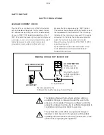
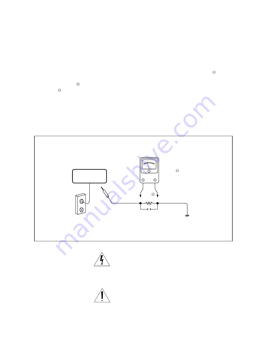
Plug the AC line cord directly into a 120V AC outlet (do

not use an isolation transformer for this check). Use an

AC voltmeter, having 5000    per volt or more sensitivity.

Connect a 1500    10W resistor,paralleled by a 0.15uF

150V AC capacitor between a knomn good earth ground

(water pipe, conduit, etc.) and all exposed metal parts of

cabinet (antennas, handle bracket, metal cabinet

screwheads, metal overlays, control shafts, etc.).

SAFTY PRECAUTIONS

LEAKAGE CURRENT CHECK

Measure the AC voltage across the 1500    resistor.

The test must be conducted with the AC switch on and

then repeated with the AC switch off. The AC voltage

indicated by the meter may not exceed 0.3V.A reading

exceeding 0.3V indicates that a dangerous potential

exists, the fault must be located and corrected.

Repeat the above test with the DVD VIDEO PLAYER

power plug reversed.

NEVER RETURN A DVD VIDEO PLAYER TO THE

CUSTOMER WITHOUT TAKING NECESSARY

CORRECTIVE ACTION.

READING SHOULD NOT EXCEED 0.3V

DVD VIDEO PLAYER

AC OUTLET

AC VOLTMETER

Test all exposed metal.
Voltmeter Hook-up for Leakage Current Check

0.15uF 150V AC

1500
10W

(5000    per volt
or more sensitivity)

Good earth ground
such as a water pipe,
conduit, etc.

The lightning flash with arrowhead symbol, within an
equilateral triangle, is intended to alert the user to the
presence of uninsulated "dangerous voltage" within the
product's enclosure that may be of sufficient magnitude to
constitute a risk of electric shock to persons.

The exclamation point within an equilateral triangle is
intended to alert the user to the presence of important
operating and maintenance (servicing) instructions in the
literature accompanying the appliance.

2-3

Summary of Contents for FWM9000

Page 1: ...umer Electronics B V Eindhoven The Netherlands All rights reserved No part of this publication may be reproduced stored in a retrieval system or transmitted in any form or by any means electronic mechanical photocopying or otherwise without the prior permission of Philips Published by LX 1 Service Audio Printed in The Netherlands Subject to modification Version 1 Seu Mini Hi Fi System FWM9000 Key ...

Page 2: ... BOARD LATAM mic BOARD mcu BOARD FWM9000 55 tuner BOARD cd BOARD 55 Location of PC Boards Technical Specification and Connection Facilities C M C M C M C M C M C M 3CD PART Top key Board ARGENTINA x 77 x 78 x 77 x 78 BRAZIL Switch Power BOARD M C M C M C M C M C M C M C M C M C M C M C M C M C M C M M M C M C M Main Board Tuner Board Amp Board Switch power Board VFD Board EQ Board Light Board Usb ...

Page 3: ...T 5 AUDIO SIGNAL SPECICFICATION 5 6 GENERAL PART 6 AUDIO SIGNAL SPECICFICATION 6 7 GENERAL PART 7 CLOCK TIMER SPECICFICATION 7 8 GENERAL PART 8 USB SD Card SPECICFICATION 8 9 GENERAL PART 9 TUNER SPECICFICATION All 9 10 GENERAL PART 10 CD MP3 SPECICFICATION 10 11 GENERAL PART 11 Ipod SPECICFICATION 11 12 GENERAL PART 12 Microhone SPECICFICATION 12 13 GENERAL PART 12 VERSION OVERVIEW SPECICFICATION...

Page 4: ...ensions with Boxes wxhxd 265mm X 382mm X 345mm DATE 11 A4 11 SH 190 1 NAME KT CHECK GENERAL PART 1 FRONT PANNEL SPECICFICATION Issued Date 12 Feb 09 Material HIPS ABS POM V2 SAN Finshing Chrome Plate Remarks Diemensions without Boxes wxhxd 1250mm X 340mm X 495 Units in Masstercarton 1 used into Class No 2 3 Remark 1 FWM9000 All Version Ver ...

Page 5: ...INET Diemensions with Boxes wxhxd 265mm X 382 mm X 345 mm n o t r a c r e l a e D n i s t i n U g K 6 2 y r e t a b g n i k c a p e v i s u l c x e t h g i e W Diemensions without Boxes wxhxd 1250mm X 340mm X 495mm Finshing Chrome Plate n o t r a c r e t s s a M n i s t i n U g K 5 8 g n i k c a p e v i s u l c n i t h g i e W Material HIPS 10 DATE NAME 10 KT CHECK SH 190 2 A4 ...

Page 6: ... 5W Ref to CRS Ref to CRS Maximum 0 5W Quality 0 8 Major 2 0 Mirror W 0 5 2 T U P N I A M O N d e t a r P 8 1 1W DEMO mode OFF NOM A INPUT S R C o t f e R S R C o t f e R W 1 y a l p s i d h t i w y b d n a t S POWER CONSUMPTION 12 05 55 77 78 98 61 93 37 Voltage Selection Frequency 0 2 0 5 5 N E 3 1 0 5 5 N E 5 6 0 0 6 N E 2 1 05 EN 55013 EN 55020 EN 60065 EN 60065 MODERATE climates N A till N A ...

Page 7: ... 5 5 r o f V 5 2 V 5 1 m i L V 2 r o N AUX Subwoofer L R 8 Ohm x2 at 40HZ to 100HZ Rear L R 4 Ohms X2 at 200Hz to 16 KHz Remarks OUTPUT POWER 1 At THD 10 Measured with 20Hz 20KHz filter Per Channel measuremend L R channel 300W Lim 1dB Power output RMS Power output RMS 1 Measurement output power just connect 2 channel loads Tuner output Lim 6dB Rated Impedance FRONT L R 8 Ohms X2 at 40Hz to 16 KHz ...

Page 8: ...urce with the following set conditions Inject sine wave 500mV at 1 KHz to L R channels of AUX IN socket Set DSC to JAZZ Flat mode and switch off DBB Frequency Refence level for DSC s without DBB on 1W Refence level for DSC S with DBB on 1 2V at the speaker terminal 4 For FWM998 Subwoofer in put 500mW 60HZ 3R Main computer Inject sine wave 500mV 2 4V to AUX IN socket with frequencies indicated in T...

Page 9: ... dB 0 dB The VEC modes are software controlled by switching the combination between DBB and DSC modes as show in Table 4 Set DSC to JAZZ Flat mode and switch of DBB OSM INCREDIBLE SURROUND Adjust volume level to obtain 1W across 3 OHM load at L R speaker output 15 dB Table 3 Tolerence 3 dB LEFT RIGHT LEFT RIGHT 60 Hz The 1W level will be used as 0 dB reference Max ON VEC MODE Optimal POP Note When...

Page 10: ...INDICATORS B S U r o r e n u T r o D C e d o M p u e k a W r e m i T n o i s r e v r e h t o r o f s r h 4 2 n o i s r e v 7 3 r o f r h 2 1 g n i t t e S e m i T s k r a m e R g n i t t e S t s a L p u e k a W t a e m u l o V No of Timer Settings 1 Clock Accuracy TECHNIAL DESCRIPTION SOFTWARE IMPLEMENTED CLOCK TIMER FUNCTION WITH 12MHZ QUARTZ OSCILLATOR GENERAL PART r e m i T d n a k c o l C g n ...

Page 11: ... i f z H K 1 h t i w B d 5 4 z H K 1 B d 0 k l a t s s o r C l e n n a h C Specification Specification Channel Crosstalk 0 dB 1 KHz d e t h g i e w A A B d 5 5 z H K 1 B d 0 o i t a R e s i o N o t l a n g i S Channel Unbalance 0 dB 1 KHz 2 z h K 1 B d 0 e s i o N D H T d e t h g i e w A B d 5 5 d e t h g i e w A z H k 1 B d 0 o i t a R e s i o N o t l a n g i S Channel Crosstalk 0 dB 1 KHz 45dB 0...

Page 12: ...ion 8 1 z H k 3 Crosstalk RF1mV Freq Dev 40kHz 25 24 30 IF 10 7 450 IF 46 49 dBf 0 03 MHz Search Tuning Sensitivity α26 10 dB A M t i n U t i n U t i m i L m o N Distortion RF 50mV M 80 3 5 Stereo 46 dB Quieting Amplification Reverse 4 B d 4 2 AM FRAME ANT 18 1 uH with shielding INDICATORS VFD Distortion RF 1mV Frq Dev 75 kHz 2 3 AGC Figure of Merit 30 25 dB F M dB 3 dB Limiting Point 17 23 5 dBf ...

Page 13: ...00 All Version Ver A 8 s i s s a h c b u S f o 1 1 O N T t c e f e d e l b i d u a o N t n i r p r e g n i F 0 6 9 4 2 9 9 0 4 0 1 7 c s i d m u 0 0 2 f o 4 2 1 O N T m u 0 0 2 m u 0 5 1 c i r t n e c c E REMARKS THD 10KHz 20dB 1 c s i d t s e T l a c i p y T mV dBA 4 dBA 1 Amplification reserve for CD 2dB 2dB Ref Level for CD is a 0dB track instead of a 6dB track dB Crosstalk 1kHz A weighted 0 9 ...

Page 14: ...R e s i o N o t l a n g i S Frequency Response 125 Hz 16 kHz 5 dBA V m 0 0 9 0 0 5 y t i v i t i s n e s t u p n i Signal to Noise Ration A weighted 1 V Charge Supply Voltage DC 5V 800mA only Ipod 3 2 FWM9000 All Version 08 09 2011 1 A4 Remark iPOD SPECICFICATION Class No Ver Issued Date 2 All speaker R channel connect to equipment for measurement All speaker L channel connect to equipment for mea...

Page 15: ... dBA V m 5 1 1 s m R n e v e l t u p n i e n o h p o r c i M dBA W m 0 2 0 5 5 S M R t u p t u o r e w o P e n o h p o r c i M A N z H K 1 B d 0 N A Channel Unbalanceo about mic1 and mic2 A N z H 3 6 B d 0 k l a t s s o r C l e n n a h C 1 3 A N e c n a t s i s e R t u p t u O Specification 8 6 x a m l o v z h K 1 B d 0 e s i o N D H T Output Voltage RL 33 k ohm dB 1 Khz Nom Lim Unit GENERAL PART ...

Page 16: ... JST XH 2P Side 300 Ohm Dipole Loop Sagami 18 1uH 100kHz 10kHz 120V 60Hz No 79 AUST NZ EN60065 CLASS II No IEC IEC No 05 12 EUROPE EN60065 SEMKO DEMKO NEMKO SEV BS415 UK EN55013 EN55020 No 75 Ohm Coaxial JST XH 2P Side 75 Ohm Pigtail Loop Sagami 18 1uH 230V 50Hz IEC IEC No No FM 87 5 108MHz MW 531 1602kHz 50kHz 9kHz 75 Ohm Coaxial JST XH 2P Side 75 Ohm Pigtail Loop Sagami 18 1uH IEC IEC FM 87 5 10...

Page 17: ...llegato allo stesso potenziale che quello della massa dell apparecchio tramite un braccialetto a resistenza Assicurarsi che i componenti e anche gli utensili con quali si lavora siano anche a questo potenziale Pour votre sécurité ces documents doivent être utilisés par des spécia listes agréés seuls habilités à réparer votre appareil en panne GB Safety regulations require that the set be restored ...

Page 18: ...perates properly after replacement if it was subject to electrostatic discharge during replacement its life might be shortened When replacing use a conductive mat soldering iron with ground wire etc to protect the laser diode form damage by static electricity And also the LSI and IC are same as above Soldering iron with ground wire or ceramic type Ground conductive wrist strap for body Conductive ...

Page 19: ...sts the fault must be located and corrected Repeat the above test with the DVD VIDEO PLAYER power plug reversed NEVER RETURN A DVD VIDEO PLAYER TO THE CUSTOMER WITHOUT TAKING NECESSARY CORRECTIVE ACTION READING SHOULD NOT EXCEED 0 3V DVD VIDEO PLAYER AC OUTLET AC VOLTMETER Test all exposed metal Voltmeter Hook up for Leakage Current Check 0 15uF 150V AC 1500 10W 5000 per volt or more sensitivity G...

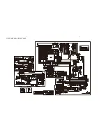
Page 20: ...R IIC PCM BCK LRCK DATE PCM CD L R TUNER L R CONTROL DATA CD PCM BCK LRCK DATE TDA8954 1 SE FUNCTION IC TDA7468D 3CD LOADER TDA8954 1 BTL SUB R 2 150W 1 300W USB2 PLAY LED DRIVER BU2090F IIC MP3 LINE USB CHANGE FFE1 1S CD DOOR MOTOR SWITCH POWER SUPPLY DC 39V Main Supply Voltage support Dock DCK3060 AC CORD CD Board MCU Board MIC Board USB Board AMP Board MAIN Board POWER Board VFD Display VFD Boa...

Page 21: ...WIRING DIAGRAM 4 1 4 1 ...

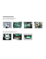
Page 22: ...A B C D Rear Portion 1 Remove 10 screws A and 8 screws B C as indicated to loosen the outer plate Front Portion Bottom Portion 3CD Part ...

Page 23: ...3 Remove 3 screws C and 4 screws E as indicated to loosen the Amp Board 4 Remove 6 screws F as indicated to loosen the AC power Board 5 Remove screws G and H as indicated to loosen the MIC KEY USB LED SW Board H J I 6 Remove 3 screws I as indicated to loosen the VFD Board 7 Remove Top panel and 6 screws J as indicated to loosen the Top key Board ...

Page 24: ...CIRCUIT DIAGRAM MAIN BOARD 6 1 6 1 ...

Page 25: ...VSSA 2 SGND 3 VDDA 4 IN2 5 IN2 6 MODE 7 OSC 8 IN1 9 N1 10 D AG1 11 OSCREF 12 D AG2 13 PROT 14 VDDP1 15 BOOT1 16 OUT1 17 VSSP1 18 STAB1 19 NC 20 VSSP2 21 OUT2 22 BOOT2 23 VDDP2 24 VSSD U702 TDA8954TH C785 104 C787 104 C786 104P C784 15N C783 15N R761 10R R762 10R C790 220P C792 220P C796 100N R765 22R C798 100N R763 22R L703 15UH L704 15UH C781 104P C780 104 C782 104 C778 224 C779 47PF C777 473 C77...

Page 26: ...707 A D 556 6 5 7 8 U707 B R776 NC C7105 22 R771 7K R770 10K C7112 7 R780 5 6K C7111 474 R779 5 6K R777 220 R778 220 C7110 330PF R781 8k2 C7113 330PF R782 1K C7190 330PF 1 VSSA 2 SGND 3 VDDA IN2 5 IN2 6 MODE 7 OSC 8 IN1 9 IN1 10 DIAG1 11 OSCREF 12 DIAG2 13 PROT 1 VDDP1 15 BOOT1 16 OUT1 17 VSSP1 18 STAB1 19 NC 20 VSSP2 21 OUT2 22 BOOT2 23 VDDP2 2 VSSD U705 TDA895 TH C7191 330PF C7202 104 C7204 104 ...

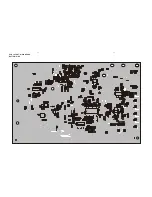
Page 27: ...PCB LAYOUT MAIN BOARD TOP SIDE 6 4 6 4 ...

Page 28: ...PCB LAYOUT MAIN BOARD BOTTOM SIDE 6 5 6 5 ...

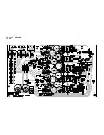
Page 29: ...PCB LAYOUT AMP BOARD TOP SIDE 6 6 6 6 ...

Page 30: ...PCB LAYOUT AMP BOARD BOTTOM SIDE 6 7 6 7 ...

Page 31: ...CIRCUIT DIAGRAM DISPLAY BOARD 7 1 7 1 ...

Page 32: ...PCB LAYOUT DISPLAY KEY BOARD TOP SIDE 7 2 7 2 ...

Page 33: ...PCB LAYOUT DISPLAY KEY BOARD BOTTOM SIDE 7 3 7 3 ...

Page 34: ...CIRCUIT DIAGRAM TUNER BOARD 8 1 8 1 ...

Page 35: ...PCB LAYOUT TUNER BOARD 8 2 8 2 ...

Page 36: ...CIRCUIT DIAGRAM MCU BOARD 9 1 9 1 ...

Page 37: ...BE 2 DATA 3 CP 4 G0 5 G1 6 G2 7 G3 8 GND 16 VCC 15 OE 14 G4 13 G5 12 G6 11 G7 10 QS1 9 QS2 IC505 74HC4094 R588 100R R564 1K R565 1K 1 3 2 SW501 R577 0R R576 0R L544 100UH C546 104 C548 104 C547 220u 16v C578 220u 16 Q523 OR3401A C565 104 R582 100k R584 2k2 3 1 2 Q522 BC817 25 3 2 Q501 BC807 25 C568 104 R528 10k C534 470P C533 470P C535 3U3 50v C536 3U3 50v R537 3K3 R536 3K3 R531 2K2 R533 2K2 C531 ...

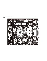
Page 38: ...PCB LAYOUT MCU BOARD 9 3 9 3 ...

Page 39: ...PCB LAYOUT CD BOARD TOP SIDE 9 4 9 4 ...

Page 40: ...PCB LAYOUT CD BOARD BOTTOM SIDE 9 5 9 5 ...

Page 41: ...10 1 10 1 EXPLODED VIEW ...

Reviews: