1 - 8
0
0
60 Hz(SUB)
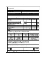
2 ) DBB ( Dynamic Bass Boot )
Set DSC to JAZZ(Flat) mode and switch off DBB,
Frequency
0
10 kHz(host computer)
0
0
2
)
B
U
S
(
z
H
0
6
POP
TECHNO
1khz (host computer)
0
0
0
1 kHz(host computer)
0
0
1khz(host computer)
0
0
0
6
0
DBB 2
20
20
DSC Modes with DBB 3 ON
JAZZ
OPTIMAL
2
-
0
OPTIMAL
1khz(SUB)
0
0
0
0
0
0
1 kHz(SUB)
0
2
2
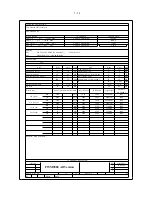
Tabel 1b ( Tolerance ± 3dB )
16
10 kHz (host computer)
0
0
4
Tabel 1a ( Tolerance ± 3dB )
1K((SUB)
0
1khz(SUB)
0
Tabel 1b ( Tolerance ± 3dB )
0
60 Hz (SUB)
10
16
60 Hz (SUB)
4
0
0
0
POP
TECHNO
JAZZ
POP
TECHNO
2
-4
0
OPTIMAL
6
-4
10 kHz (host computer)
0
OPTIMAL
2
0
6
0
0
1 kHz (host computer)
0
2
0
4
16
0
13
0
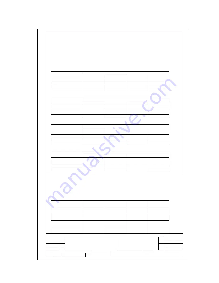
DSC Modes with DBB 2 ON
4
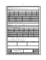
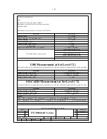
AUDIO SIGNAL PROCESSING
MP3-USB Mini Hi Fi System with Digital Tuner , 3 CDC-MP3,(Main:2×350W+Rear:2×150W+SUB:2x300W) Universal Class D Power Amplifier
1 ) DSC ( Digital Sound Control )
Select AUX as input source with the following set conditions:
Inject sine wave 500mV at 1 KHz to L/R channels of AUX-IN socket.
Set DSC to JAZZ(Flat) mode and switch off DBB.
Frequency
Refence level for DSC's without DBB on=1W.
Refence level for DSC'S with DBB on=1.2V at the speaker terminal .
4
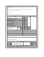
For FWM998 Subwoofer in put 500mW 60HZ @ 3R (Main computer )
Inject sine wave 500mV-2.4V to AUX-IN socket with frequencies indicated in Table 1.
60 Hz (SUB)
DSC Modes with DBB Off
JAZZ
POP
TECHNO
08-09-2011
GENERAL PART 1 - GENERAL SPECICFICATION
0
0
0
10K Hz(host computer)
Issued Date
10 kHz(host computer)
0
2
Tabel 1b ( Tolerance ± 3dB )
8
12
Frequency
DBB 3
Frequency
DSC Modes with DBB 1 ON
0
2
8
8
DBB 1
0
1 Hz(SUB)
0
1 kHz (host computer)
0
Frequency
DBB OFF
JAZZ
2
Reference level for the test is 500mW on the speaker terminals.
Tabel 2 of FWM998( Tolerance ± 3dB )
Select AUX as input source with the following set conditions :
Inject sine wave 500mV at 1kHz to L/R channels of AUX - IN socket.
0
0
0
A4
Class No
FWM9000 All Version
Ver
2
1
SH 190 - 5
KT
CHECK
3
DATE :
NAME : Andy Lai
10
10
Summary of Contents for FWM9000
Page 21: ...WIRING DIAGRAM 4 1 4 1 ...
Page 24: ...CIRCUIT DIAGRAM MAIN BOARD 6 1 6 1 ...
Page 27: ...PCB LAYOUT MAIN BOARD TOP SIDE 6 4 6 4 ...
Page 28: ...PCB LAYOUT MAIN BOARD BOTTOM SIDE 6 5 6 5 ...
Page 29: ...PCB LAYOUT AMP BOARD TOP SIDE 6 6 6 6 ...
Page 30: ...PCB LAYOUT AMP BOARD BOTTOM SIDE 6 7 6 7 ...
Page 31: ...CIRCUIT DIAGRAM DISPLAY BOARD 7 1 7 1 ...
Page 32: ...PCB LAYOUT DISPLAY KEY BOARD TOP SIDE 7 2 7 2 ...
Page 33: ...PCB LAYOUT DISPLAY KEY BOARD BOTTOM SIDE 7 3 7 3 ...
Page 34: ...CIRCUIT DIAGRAM TUNER BOARD 8 1 8 1 ...
Page 35: ...PCB LAYOUT TUNER BOARD 8 2 8 2 ...
Page 36: ...CIRCUIT DIAGRAM MCU BOARD 9 1 9 1 ...
Page 38: ...PCB LAYOUT MCU BOARD 9 3 9 3 ...
Page 39: ...PCB LAYOUT CD BOARD TOP SIDE 9 4 9 4 ...
Page 40: ...PCB LAYOUT CD BOARD BOTTOM SIDE 9 5 9 5 ...
Page 41: ...10 1 10 1 EXPLODED VIEW ...

