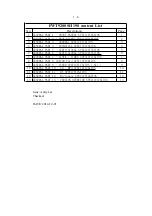
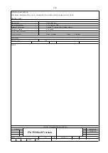
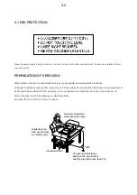
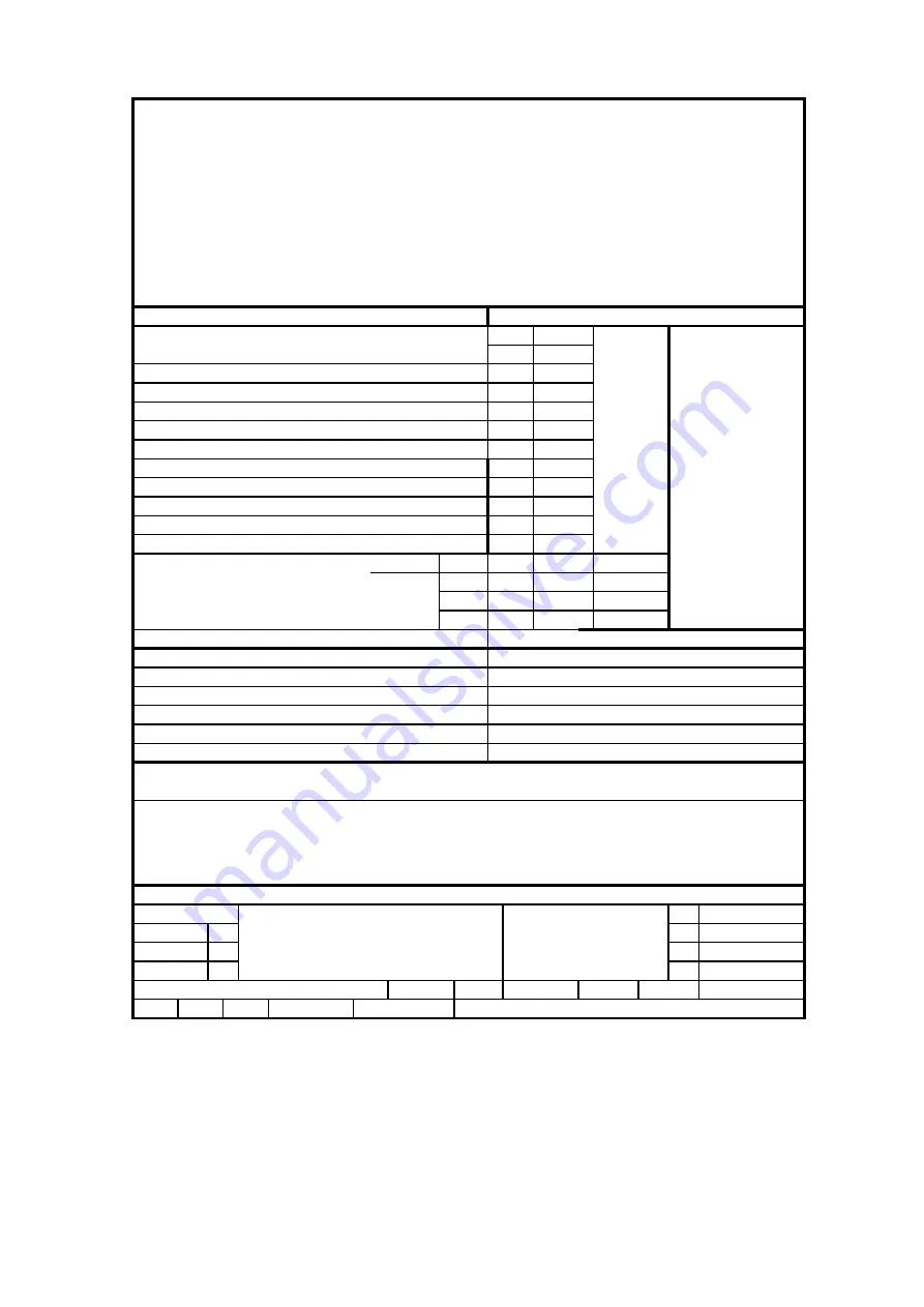
A4
CHECK
DATE :
NAME : Andy Lai
12
9
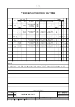
SH 190 -9
21-Dec-12
2
Issued Date
1
Class No
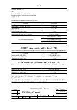
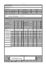
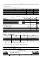
FWT9200 All Version
Ver
3
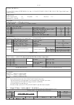
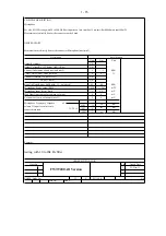
testing with 20 to 20k Hz filter
USB SPECICFICATION
Remarks :
dB
Microphone Frequency response at
volume 23,input leven 1mv rms,
connect main load
)/)5FK
dB
.+=
ref
dB
.+=
±3
mV
Vol.min=vol1.(mic vol min,main vol 1)
2
4
mV
±4
Max Hum Noise(mic vol max,main vol max)
6
8
+=
45
40
dBA
Microphone input leven ( Rms)
1
1.5
mV
dBA
Microphone Power output( RMS )
550
+/- 20%
mW
( 0 dB, 1 KHz )
N/A
Signal to Noise Ratio ( 0dB,1kHz ) ( A - weighted )
Channel Crosstalk ( ( 0 dB, 63Hz ) )
N/A
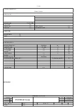
Specification
THD + Noise ( 0dB, 1Khz )vol max
6
8
%
Output Voltage RL = 33 k ohm ( )dB, 1 Khz )
N/A
Channel Unbalanceo about( mic1 and mic2)
Output Resistance
N/A
1
+/- 3
Nom
Lim
Unit
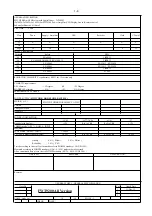
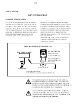
GENERAL PART
Measurement are directly done at the connector Microphone(mic1,mic2)
Description
TECHNIAL DESCRIPTION
Microphone
See also SH 190 testing with 20 to 20k Hz filter,input leven 1mv rms(lim:1.5mv rms) Rs=600ohm output 500mW
Measurment are directly done at the coonector on the board
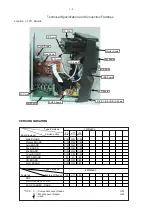
1 - 15
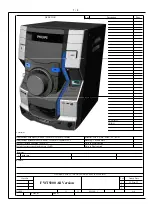
Summary of Contents for FWT9200 Series
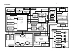
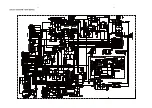
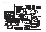
Page 22: ...WIRING DIAGRAM 4 1 4 1 ...
Page 24: ......
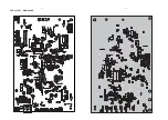
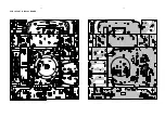
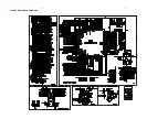
Page 25: ...6 2 6 2 PCB LAYOUT MAIN BOARD ...
Page 26: ...7 1 7 1 CIRCUIT DIAGRAM DISPLAY BOARD ...
Page 27: ...PCB LAYOUT DISPLAY BOARD 7 2 7 2 ...
Page 29: ...8 2 8 2 PCB LAYOUT CD BOARD ...
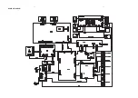
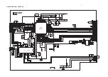
Page 30: ...CIRCUIT DIAGRAM MCU BOARD 9 1 9 1 ...
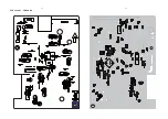
Page 31: ...PCB LAYOUT MCU BOARD 9 2 9 2 ...
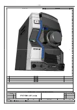
Page 34: ...PCB LAYOUT AMP BOARD 10 3 10 3 ...
Page 35: ...CIRCUIT DIAGRAM TUNER BOARD 11 1 11 1 ...
Page 36: ...PCB LAYOUT TUNER BOARD 11 2 11 2 ...
Page 37: ...12 1 12 1 EXPLODED VIEW ...