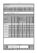
+2.0 dB
- 1.0 dB
-
2V
-
0
-
2V
-
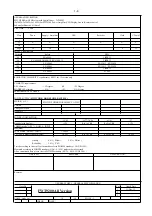
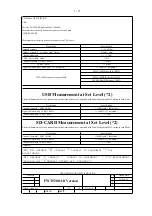
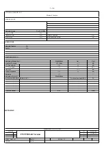
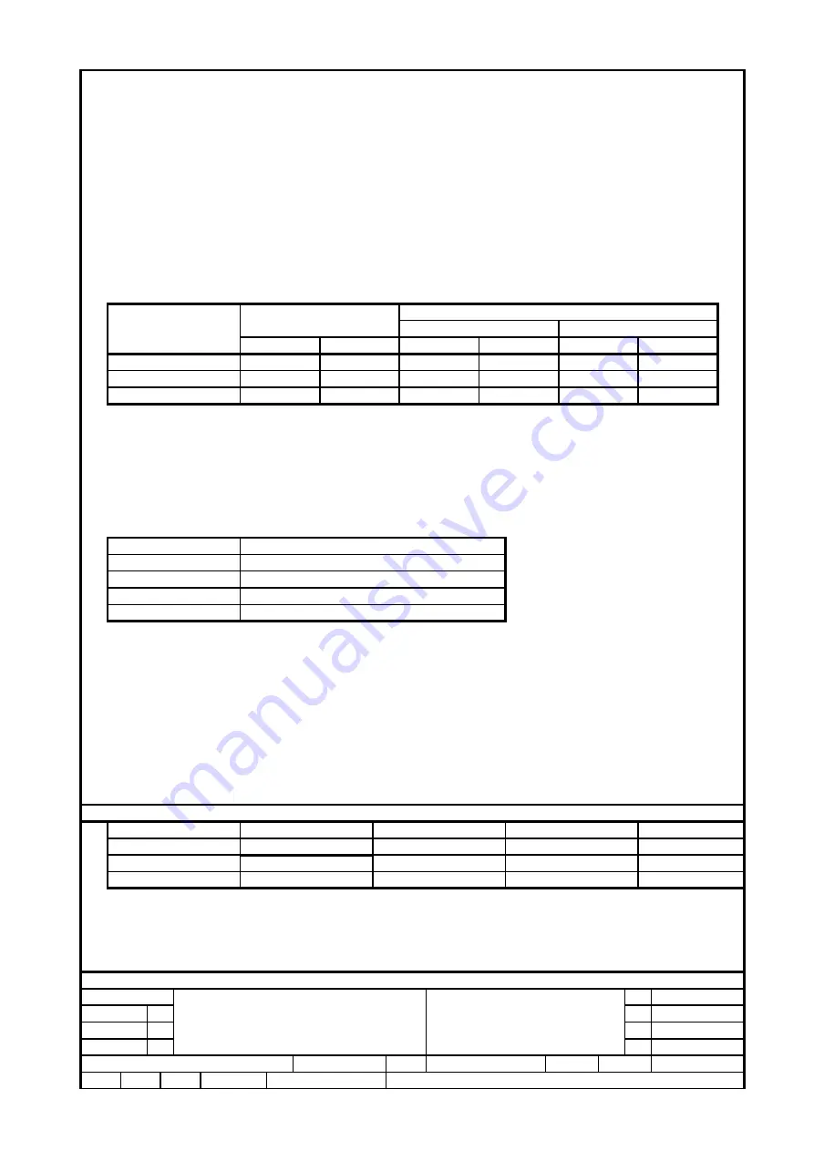
Set DSC to JAZZ ( Flat ) mode and switch of DBB, OSM & INCREDIBLE SURROUND.
Adjust volume level to obtain 1W across 3 OHM load at L/R speaker output.
Inject sine wave 2V to AUX-IN socket withfrequency indicated in Table 3 (input level 600mV for /37,2V for /55 ).
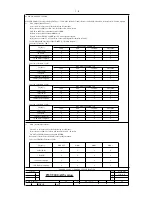
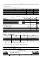
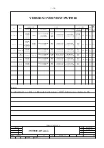
4 ) DSC Mode ( Jazz , Rock, Techno and Optimal )
- 0.5 dB
-
+ 3.0 dB
-5 dB
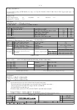
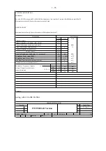
Select AUX as input source.
Inject sine wave 2V at 1kHz to AUX-IN socket, two channel at a time (input level 600mV for /37,2V for /55 ).
LEFT
RIGHT
OUTPUT LEVEL
IS OFF
IS ON
10 kHz
Note : The above specs also apply to right channel.
1 kHz
AUDIO SIGNAL PROCESSING
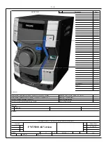
MP3 - USB Mini Hi Fi System with Digital Tuner , 3 CDC-MP3, (Main:2×360W+SUB:2×360W+Rear:2x180W) Universal Class D Power Amplifier
FREQ
INPUT LEVEL
3 ) IS ( Incredible Sound )
2V
-
DBB 2
+ 3.5 dB
0 dB
The VEC modes are software controlled by switching the combination between DBB and DSC modes
as show in Table 4.
Set DSC to JAZZ ( Flat ) mode and switch of DBB, OSM & INCREDIBLE SURROUND.
Adjust volume level to obtain 1W across 3 OHM load at L/R speaker output.
- 15 dB
Table 3 ( Tolerence ± 3 dB )
LEFT
RIGHT
LEFT
RIGHT
60 Hz
Max ON
VEC MODE
Optimal
POP
Jazz
10 kHz
-1
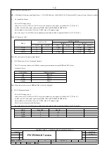
Inject sine wave 2V to AUX-IN socket withfrequency indicated in Table 5 (input level 600mV for /37,2V for /55 ).
Note : When these modes are activ DBB and DSC will not be displayed
DBB Level preset
DBB OFF
DBB 3
Techno
DBB 3
The 1W level will be used as 0 dB reference
5 ) MAX ( Maximum Sound )
Select AUX as input source.
Inject sine wave 2V at 1kHz to AUX-IN socket, one channel at a time (input level 600mV for /37,2V for /55 ).
FREQ
Max OFF
DATE :
NAME : Andy Lai
10
10
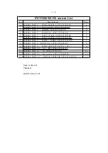
SH 190 - 6
+19
3
1
-1
1 kHz
0
CHECK
GENERAL PART 1 - AUDIO SIGNAL SPECICFICATION ( 2 )
Class No
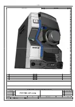
FWT9200 All Version
Ver
Issued Date
A4
2
1 - 9
21-Dec-12
60 Hz
Summary of Contents for FWT9200 Series
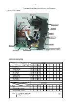
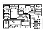
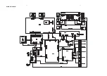
Page 22: ...WIRING DIAGRAM 4 1 4 1 ...
Page 24: ......
Page 25: ...6 2 6 2 PCB LAYOUT MAIN BOARD ...
Page 26: ...7 1 7 1 CIRCUIT DIAGRAM DISPLAY BOARD ...
Page 27: ...PCB LAYOUT DISPLAY BOARD 7 2 7 2 ...
Page 29: ...8 2 8 2 PCB LAYOUT CD BOARD ...
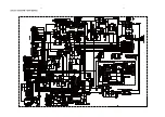
Page 30: ...CIRCUIT DIAGRAM MCU BOARD 9 1 9 1 ...
Page 31: ...PCB LAYOUT MCU BOARD 9 2 9 2 ...
Page 34: ...PCB LAYOUT AMP BOARD 10 3 10 3 ...
Page 35: ...CIRCUIT DIAGRAM TUNER BOARD 11 1 11 1 ...
Page 36: ...PCB LAYOUT TUNER BOARD 11 2 11 2 ...
Page 37: ...12 1 12 1 EXPLODED VIEW ...