background image

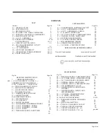
CONTENTS 

TEXT 

Section 

Page No. 

UNIT LOCATION 

Unit 

Page No. 

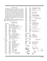
 INTRODUCTION 

 CONVERGENCE ASSEMBLY LAYOUT 

17 

 SPECIFICATION 

 L.O.P.T. ASSEMBLIES

UPPER 

18 

 RECEIVER NOTES 

 L.O.P.T. ASSEMBLIES

LOWER 

18 

 625-LINE V.H.F. RELAY OPERATION 

 T.B. PANEL

PRINT SIDE 

20 

 SPECIALLY MOUNTED COMPONENTS 

 C.R.T. BASE PANEL

COMPONENT SIDE 

21 

 MAINTENANCE NOTES 

 CHROMA. PANEL

PRINT SIDE 

22 

 L.O.P.T. ASSEMBLY 

6-7 

 CENTRE CHASSIS WIRING 

25 

PRESET ADJUSTMENTS 

9-10 

 TOP LEFT CHASSIS WIRING 

25 

-  

CONVERGENCE 

10-11 

 SUB-ASSEMBLIES WIRING 

26 

 GREY SCALE TRACKING 

12 

 LOWER CHASSIS WIRING 

26 

 COLOUR DIFFERENCE OUTPUT 


 I.F. PANEL

COMPONENT SIDE 

27 

ADJUSTMENTS 

12 


 I.F. ALIGNMENT 

12-14 

EXPLANATION OF WIRING CODING 


 DECODER ALIGNMENT 

14-15 


 INTEGRATED TUNER ASSEMBLY 

32-35 

On unit J, lead marked 

is connected to unit K 

0 — 

SPARE PARTS LIST 

37-43 


and there marked 

. Similarly, on unit D, lead marked 

is connected to unit E and there marked 

ILLUSTRATIONS 

Fig. No. 

RECEIVER IDENTIFICATION 

 SPRING RESISTOR R1073 

I f 2  

  C O N V E R G E N C E   C O V E R   3 


ASSEMBLY OF C.R.T. AND SHIELD 4 


C.R.T. SHIELD 5 

 TRIM PLAN 

 THIRD HARMONIC TUNING 

 DEFLECTION ASSEMBLY 

 CONVERGENCE PANEL 

 TERMINATING PAD 

10 

 DAMPER/DETECTOR UNIT 

11 

 DETECTOR UNIT 

12-15 RESPONSE CURVES 
16 

 BIAS NETWORK 

17 

 X-Y DISPLAYS 

18 

 BLOCK DIAGRAM 

19 

 CONVERGENCE ASSEMBLY WIRING 

20 

 L.O.P.T. ASSEMBLY

UPPER 

21 

 L.O.P.T. ASSEMBLY

LOWER 

22 

 L.O.P.T. PANEL 

23 

 TIME BASE PANEL

PRINT SIDE 

Page No. 


10 
11 
12 

12 

12 

14 

14 

15 
16 

17 

18 

18 

19 
20 

Fig. No. 

24 

 TIME BASE PANEL

COMPONENT SIDE 

25 

 C.R.T. BASE PANEL

COMPONENT SIDE 

26 

 C.R.T. BASE PANEL

PRIPANEL-PRINT 

27 

 CHROMA. PANEL

PRINT SIDE 

28 

 CHROMA. PANEL

COMPONENT SIDE 

29 

 CAN ASSEMBLIES

A TO F 

30 

 CHASSIS WIRING

CENTRE AND 

TOP LEFT 

31 

 CHASSIS WIRING

LOWER, AND 

SUB-ASSEMBLIES 

32 

 I.F. PANEL

COMPONENT SIDE 

33 

 I.F. PANEL

PRINT SIDE 

34-36 VOLTAGE WAVEFORMS 
37 

 TUNER MECHANISM

EXPLODED 

VIEW 

38 

 DRIVE GEAR SETTING 

39 

 TUNER

COMPONENT LAYOUT 

40 

 TUNER

CIRCUIT DIAGRAM 

41 

 CIRCUIT DIAGRAM

I.F., etc. 

42 

 CIRCUIT DIAGRAM

T.B., etc. 

Page No. 

21 
21 

21 

22 

23 
24 

25 

26 

27 

28 

29-31 

32 

33 
34 

35 

In 

pocket 

Page One 


Summary of Contents for G22K511

Page 1: ...VERS c es C O MMB I N E D E L E C T R O NI C S ER V I C ES LI MI TE D 604 PURLEY WAY WADDON CROYDON CR9 4DR TELEPHONES Spare part orders 01 686 3831 General service enquiries 01 688 7722 After business hours Recorded messages on both lines Telex 262308 AUGUST 1969 Please quote CES 739 when ordering further copies CES 739 ...

Page 2: ...d ILLUSTRATIONS Fig No RECEIVER IDENTIFICATION 1 SPRING RESISTOR R1073 If2 CONVERGENCE COVER 3 ASSEMBLY OF C R T AND SHIELD 4 C R T SHIELD 5 TRIM PLAN 6 THIRD HARMONIC TUNING 7 DEFLECTION ASSEMBLY 8 CONVERGENCE PANEL 9 TERMINATING PAD 10 DAMPER DETECTOR UNIT 11 DETECTOR UNIT 12 15 RESPONSE CURVES 16 BIAS NETWORK 17 X Y DISPLAYS 18 BLOCK DIAGRAM 19 CONVERGENCE ASSEMBLY WIRING 20 L O P T ASSEMBLY UP...

Page 3: ...G22K511 G25K512 Page Two ...

Page 4: ...T2144 BC148 T2145 BC148 T2146 BC148 T2147 BC148 T2624 BF197 T2755 BF173 T3401 BF180 T3402 BF182 T3403 BF183 T3495 BC108 T7011 BF195 T7012 BF195 T7013 BF194 T7014 BF194 T7015 BC107 X1101 BY127 X1102 BY127 X1103 BA148 X1104 BA148 X1105 BYX10 X1106 BA148 X1292 BA148 X1293 BA148 X1294 BA148 X2151 0A91 X2152 BA154 X2153 0A91 X2530 AA119 X2531 AA119 X2625 0A90 X2756 0A90 X3496 BZY88 X4140 BA148 X4141 BA...

Page 5: ...l trimming tool A special star shaped trimming tool is necessary for the alignment of the tuner I F coil and also for adjustment of certain other cores This trimming tool is available as part of the Philips trimming tool kit 800 TX and engineers are advised that any attempt to adjust these cores with a non standard tool may damage them 5 Use of the circuit diagram a The complete circuit of the G6 ...

Page 6: ...under the tags and not wrapped around them 2 Ballast resistors During manufacture a high melting point solder is employed on all connections to the supply ballast resistors R1052 R1053 It is most essential that this grade of solder e g Ersin Comsol Alloy is used with a high temperature soldering iron if this component is replaced 3 Thermal fuses FS1108 and FS1110 Two thermal fuses FS1108 and FS111...

Page 7: ...hdrawn from the cabinet 7 Replacement of degaussing coils L1723 4 Remove the main chassis tuner assembly control panel and con vergence unit together with the convergence yoke deflection coils and blue lateral unit Lay the cabinet face downwards supported at each corner to prevent the C R T taking the weight of the cabinet 8 Removal of the C R T WARNING Extreme care must be taken when handling the...

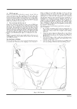
Page 8: ... all the tappings on the line trans former windings are available externally via the two 10 way sockets mounted on the side of the E H T can assembly and connections to many components can be made either on the printed panel or within the valve compartment of the assembly once the gauze screen has been removed In cases of arcing due to breakdown of a component inside the assembly it may be first n...

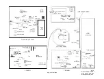
Page 9: ...2 o 0 0 0 1 0 FOCUS L L L L 2744 2746 2745 2747 PRE SET A G C c i 7 1 0 5 7 L L 72 2 3 4 2 5 2 7 8 3 L 10 0 OD 9 r gd R2092 n L L L2598 0 _____11_2596 7 2555 2554 L2564 0 L2621 L2620 L 2 5 8 6 L2773 L2775 Is F1271b 12 L 2643 4 L264 W611 R2073 A M REJECTION L2603 I 5 5 1 L 2 5 26 L2528 9 LUMINANCE FEED TO C R T CATHODE L2503 l L2504 R7285 I 1 C R T CUT OFF R1167 CONTRAST sl 75Z3 7559 60 7561 L 7 6 ...

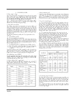
Page 10: ... picture is correctly set up Adjust R5045 for optimum focus 10 Vertical hold control R4098 Adjust vertical hold control R4098 to obtain a correctly locked picture 11 Vertical bias control R4105 Before adjusting R4105 check that the boost voltage is correct see para 2 Connect a voltmeter across R4117 pin 7 V4004 to chassis then adjust R4105 to give a reading of 12 5 volts 12 Height control R4101 Be...

Page 11: ... each control Degaussing The receiver is fitted with an automatic degaussing circuit which operates each time the set is switched on from cold However in cases where the C R T and or associated metal parts have been subjected to extra strong magnetic fields it may be necessary to pass an external degaussing coil across the C R T face and in each corner before purity convergence adjustments are car...

Page 12: ...Page Ten ...

Page 13: ...n The solder tags on L1523 are at H T potential 4 Converge the horizontal lines at the bottom of the screen with control 3 and the horizontal lines at the top of the screen with control 4 5 With controls 7 and 8 converge the left and right hand vertical lines 6 Check static convergence and readjust if necessary 7 Switch on the blue gun depress button 17 again 8 Adjust controls 10 11 and 12 to make...

Page 14: ...Page Eleven ...

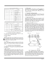
Page 15: ... warm up period of at least 20 minutes should be allowed for thermal stabi lisation of both receiver and test equipment Leads should be as short as practicable in order to have least effect on the response curve When the sweep generator is connected to the various injection points stated the terminating pad shown in Fig 9 should be used The adjustment of certain vision I F coils will affect both l...

Page 16: ...om X7326 and pins 4 and 5 of V7008 then check the adjustment of R7179 and R7206 see section H paras 22 and 23 Note When alignment of the chroma bandpass circuit has been completed the decoder alignment must be checked particularly the setting of L7559 60 and L7561 I F ALIGNMENT TABLE Inputfrom C20 4I sweep generator to and turn R2092 fully clockwise TP7 tuner injection point via the terminating pa...

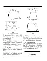
Page 17: ... normal picture Connect a high impedance voltmeter from pin 2 of V7003 to chassis ve lead to chassis Adjust L7624 6 for maximum negative reading on the meter approx 4v OVERALL CHROMINANCE BANDPASS RESPONSE 503904e Fig 13 37MHz 33 5MHz RESPONSE AT COLLECTOR T2143 503904f Fig 15 4 R7618 discriminator balance Apply a colour signal to the aerial socket and set up the controls for a normal picture Conn...

Page 18: ...ips of the duplicated ellipses o 17B shows these ellipses before the adjustment is carried out 7 Adjust L7562 3 so that the diagonal ellipses especially on the magenta green axis become as thin as possible It may not be possible to make all the ellipses into thin lines with L7562 3 in which case the best compromise should be achieved 8 Synchronise the reference oscillator by removing the 1 0v sour...

Page 19: ...Page Fifteen ...
Reviews: