background image

Published by KC-TE 06

34

 AV Systems   

Printed in the Netherlands  

Subject to modification  

EN 3139 785 31952

HTS3105MKI

/

98/75

HTS3105MKII

/

98/75

DVD Receiver

CLASS  1

LASER PRODUCT

1  Technical Specifications and Connection


Facilities 

2

2  Measurements Setup, Service Aid & 


Lead Free Requirements  

4


Service Hints 

8

3  Directions For Use 

9

4  Dismantling Instructions & Service Positions 

11

5  Service Test Program  

14

6  Block Diagram and Wiring Diagram 

17


Block Diagram 

17


Wiring Diagram 

18

7  Circuit Diagram and PWB Layout 

19 


Front: Display 

19 


Front: Display (Top view) 

20 


Front: Display (Bottom view) 

21 


Front: Standby 

22


Front: Standby Layout (Top View) 

22


Front: Standby Layout (Bottom View) 

22

MKI Mono Board: Circuit Diagram (Part 1) 

23 


MKI Mono Board: Circuit Diagram (Part 2) 

24

©Copyright 2006 Philips Consumer Electronics B.V. Eindhoven, The Netherlands.

All rights reserved. No part of this publication may be reproduced, stored in 

a retrieval system or transmitted, in any form or by any means, electronic, 

mechanical, photocopying, or otherwise without the prior permission of Philips.

Version 1.1

Contents 

Page

Contents 

Page

MKI Mono Board: Circuit Diagram (Part 3) 

25

MKI Mono Board: Circuit Diagram (Part 4) 

26

MKI Mono Board: Circuit Diagram (Part 5) 

27

MKI Layout: Mono Board (Top View) 

28

MKI Layout: Mono Board (Bottom View) 

29

MKII Mono Board: Circuit Diagram (Part 1) 

30 


MKII Mono Board: Circuit Diagram (Part 2) 

31

MKII Mono Board: Circuit Diagram (Part 3) 

32

MKII Mono Board: Circuit Diagram (Part 4) 

33

MKII Mono Board: Circuit Diagram (Part 5) 

34

MKII Layout: Mono Board (Top View) 

35

MKII Layout: Mono Board (Bottom View) 

36 


PSU Circuit Diagram 

37

8  Overview - Modulator, Input/Output and  


Headphone/Line Output Connectors 

38


TAS5086-5142V6REF 

38


Power Output Stage (BTL) 

39


Power Supplies 

40


Amp Board Layout : Topview 

41


Amp Board Layout : Bottomview 

42

9  Exploded View & Spare Parts List 

43 


Exploded View of the set 

43 


Spare Part List 

44


Revision List 

45

This Service manual is for HTS3105/98/75 First and Second Generation 

models.
For First Generation model (HTS3105/98/75), the serial number begins with 

NW1A xxxx xxxx (PSCI) and VN1A xxxx xxxx (PACH).
For Second Generation model (HTS3105/98/75), the serial number begins with 

NW2A xxxx xxxx (PSCI) and VN2A xxxx xxxx (PACH).

Summary of Contents for HTS3107

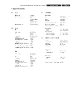
Page 1: ...ng or otherwise without the prior permission of Philips Version 1 1 Contents Page Contents Page MKI Mono Board Circuit Diagram Part 3 25 MKI Mono Board Circuit Diagram Part 4 26 MKI Mono Board Circuit Diagram Part 5 27 MKI Layout Mono Board Top View 28 MKI Layout Mono Board Bottom View 29 MKIIMono Board Circuit Diagram Part 1 30 MKIIMono Board Circuit Diagram Part 2 31 MKIIMono Board Circuit Diagr...

Page 2: ...ical Specifications and Connection Facilities LOCATION OF PC BOARDS Progressive Scan TV In Aux In Y Pb Pr YUV Component Video Output SCART Features Type Versions 98 Line Out x x x x x x CVBS HTS3105 HTS3100 _ VERSION VARIA TIONS ...

Page 3: ...Hz Grid 9kHz 10kHz IF frequency 450kHz 1kHz Aerial input Frame aerial Sensitivity at 26dB S N 4 0mV M Selectivity at 18kHz bandwidth 20dB IF rejection 45dB Image rejection 28dB Distortion at RF 50mV m 80 5 1 3 AMPLIFIER Output power Front 100W RMS channel Rear 75W RMS channel Center 100W RMS Subwoofer 150W RMS Frequency response 0 5dB 20Hz 20kHz Hum Volume Minimum 200nW Residual noise Volume Minim...

Page 4: ...s 250Hz 15kHz e g 7122 707 48001 LF Voltmeter e g PM2534 DUT S N and distortion meter e g Sound Technology ST1700B Frame aerial e g 7122 707 89001 Tuner AM MW LW To avoid atmospheric interference all AM measurements have to be carried out in a Faraday s cage Use a bandpass filter or at least a high pass filter with 250Hz to eliminate hum 50Hz 100Hz RF Generator e g PM5326 Ri 50Ω Bandpass 250Hz 15k...

Page 5: ...al Torx driver holder 4822 395 91019 Torx bit T10 150mm 4822 395 50456 Torx driver set T6 T20 4822 395 50145 Torx driver T10 extended 4822 395 50423 Compact Disc SBC426 426A Test disc 5 5A 4822 397 30096 SBC442 Audio Burn in Test disc 1kHz 4822 397 30155 SBC429 Audio Signals disc 4822 397 30184 Dolby Pro logic Test Disc 4822 395 10216 ...

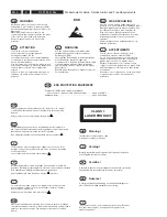
Page 6: ...la massa dell apparecchio tramite un braccialetto a resistenza Assicurarsi che i componenti e anche gli utensili con quali si lavora siano anche a questo potenziale GB ESD PROTECTION EQUIPMENT Complete Kit ESD3 small tablemat wristband connection box extention cable and earth cable 4822 310 10671 Wristband tester 4822 344 13999 CLASS 1 LASER PRODUCT GB Warning Invisible laser radiation when open A...

Page 7: ...void wear out of tips switch off un used equipment or reduce heat Mix of lead free solder alloy parts with leaded solder alloy parts is possible but PHILIPS recommends strongly to avoid mixed solder alloy types leaded and lead free If one cannot avoid or does not know whether product is lead free clean carefully the solder joint from old solder alloy and re solder with new solder alloy SAC305 Use ...

Page 8: ...t a paper clip on the flexfoil to short circuit the contacts fig 1 5 Replace the defective loader with a new loader 6 Remove paperclip from the flexfoil and connect it to the new loader 7 Remove solder joint on the ESD protection point ATTENTION The laser diode of this loader is protected against ESD by a solder joint which shortcircuits the laserdiode to ground For proper functionality of the loa...

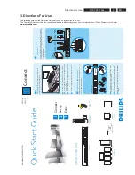
Page 9: ...ear level DVD System rear B Connect the radio antennas Keep the antennas away from the electronic devices to prevent unwanted interference A B C A Connect the FM antenna to the FM socket Extend the wire and fix its end to the wall B Unfold the AM MW loop antenna and fix the claw into the slot C Push the tabs and insert the wires into the AM MW sockets C Connect the speakers and subwoofer Connect t...

Page 10: ...re shown on the TV while operating this DVD system not for the DVD disc menu 3 Enjoy Start disc playback A Press OPEN CLOSE to open the disc tray Load a disc and close the disc tray B Playback will start automatically C If the disc menu appears use TS keys to select an option in the menu and press PLAY X to start playback D Press STOP x to stop playback Listen to radio A Press TUNER The display pa...

Page 11: ...e bottom side 2 Loosen 4 screws A See Figure 4 3 to remove the PSU Module Figure 4 3 3 Loosen 4 screws B See Figure 4 4 to remove the DVD Loader Figure 4 4 4 Dismantling Instructions 4 1 Dismantling of the DVD Loader Tray Cover 1 Insert a minus screwdriver and push the lever in the direction as shown in Figure 4 1 to unlock the tray before sliding it out Figure 4 1 2 Remove the Tray Cover as shown...

Page 12: ...er Module Mono Board 1 Loosen 1 screw to remove the Tuner Module 2 Loosen 2 screws D to remove the Mono Board Figure 4 5 AP Figure 4 6 D F 4 4 Dismantling of the Amp module Board 1 Loosen 4 screws F and 2 screws G See Figure 4 7 Figure 4 8 to remove Amp Module Board Figure 4 7 Figure 4 8 G H H ...

Page 13: ...antling Instructions Service Positions 3 4 Service Positions Service Position Front Board Service Position Amp Board Service Position Mono Board Insulation Sheet Amp Board Insulation Sheet Front Board Insulation Sheet Mono Board ...

Page 14: ... display and whether there are any short circuits open circuits or any other defects Player Following display patterns are used to test the display and its connections to μP Pattern 1 Default All display control pins are ON to check the open circuits Pattern 2 Alternate display control pins are on Test Pattern 0x55 to check the short circuits on Data port Receiver HTS3100 3105 Following display pa...

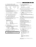
Page 15: ...ocedure to upgrade the firmware 1 Power up the set and open tray 2 Insert the prepared Upgrade CDROM and close the tray 3 The set will display LOAD MULTICH UPG END The whole process takes less than 2 minutes Note Do not press any button or interrupt the main supply upgrading process Otherwise the set may become defective 4 When the upgrade is completed the tray will close automatic 5 The tray will...

Page 16: ...EN 16 3139 785 3195x 5 Service Test Program Notes ...

Page 17: ...3139 785 3195x MONO BD 3139 248 3380x MKI 3139 248 87731 MKII 200 W Power Amplifier Front Board HEF4052B ERROR PSU CONTROL HTS3100_block_duagram_MK2 pdf_2006_04_13 6 Block Diagram Wiring Diagram Block Diagram ...

Page 18: ...FOIL 10P 120 10P AD FOLD MONO BOARD 3139 243 3380x MKI 3139 248 87731 MKII 24P 220mm FFC 1 LOAD LOAD TROUT GND 5 TRIN 5P 220mm PH 6P 180mm PH 1 SP Sp LIMIT GND SL 6 SL 4P PH BOARD IN TO FRONT MIC 3139 248 87361 FR1 2 layer 3139 248 87371 5P EH TO Front 12VA 1 MIC GND 12VA 4 1 5VL GND 5VL 5VL GND D 12VA GNDA 12VA STBY POW_DN 12VL 12 GND M 12P EH TO PSU Power Supply 3139 247 12501 3139 247 12511 1 G...

Page 19: ...11 12 Φ 8 6 7708 PT6312BLQ VFD 3725 2718 100n 10K F723 F702 100n 2716 F704 F705 100p 2700 1K2 2K2 3702 3701 SKQNAB 1713 1 2 3 1708 WH03D 1 3731 F703 3728 4K7 150R 4K7 BC847B 3740 7703 47p 2704 MGND 68K 3703 F701 F719 10u 2724 F711 F707 F730 F732 F735 F727 100n 220p 2731 2726 2717 100n 100R 3724 10p 2714 F721 F724 F720 F715 F718 1712 3730 4K7 SKQNAB SKQNAB 1711 1716 SKQNAB 2 3 4 5 F706 1703 WH05D 1...

Page 20: ...EN 20 3139 785 3195x 7 Front Display topview Circuit Diagram and PWB Layout DisplayBd_Topview_33782 pdf_031806 ...

Page 21: ...EN 21 3139 785 3195x Front Display Bottom view 7 Circuit Diagram and PWB Layout DisplayBd_Bottomview_33782 pdf_031806 ...

Page 22: ... 1801 A2 1802 A1 2801 A1 1 2 1 2 A 3801 A2 6801 B2 F803 B F801 F802 6801 LTL 816EELC 470R 1 2 3 3801 B3B EH A 1802 3139 243 33842_StdyBd_sh130_sh1 pdf_031806 2801 220p 1801 SKQNAB StdbyBd_Topview_33842 pdf_031806 StdbyBd_Bottomview_33842 pdf_031806 Front Standby Top View Front Standby Bottom View ...

Page 23: ..._3 MA DVDD3_2 80 AD0 81 AD1 82 AD2 83 AD3 84 DVSS_2 85 AD4 86 AD5 HIGHA3 73 DVDD3_1 HIGHA2 74 HIGHA1 75 76 IOA20 77 IOCS 78 IOA1 IOOE 79 8 APLLVDD3 66 IOWR A16 67 HIGHA7 68 69 HIGHA6 7 DVDRFIN 70 HIGHA5 71 HIGHA4 72 59 HIGHA0 6 DVDRFIP 60 IOA18 61 IOA19 62 DVSS_1 63 APLLCAP APLLVSS 64 65 51 TDO DVDD18_1 52 53 IOA2 54 IOA3 55 IOA4 56 IOA5 57 IOA6 58 IOA7 44 USBP USBM 45 46 USB_VDD3 FG 47 TDI 48 TMS...

Page 24: ...1 32 33 34 20 21 17 37 1M X 16 X 4 DRAM F IS42S16400A 7TLI 23 24 22 35 25 26 D 7201 8 2268 100n 3213 1 10R 1 3139 243 33803_sh130_sh2 pdf_031806 2274 22p 2279 100n 2280 100n T240 2260 22p 3211 4 4 5 4201 3 6 10R 2 7 10R 3211 3 8 10R 3211 2 3212 1 10R 1 T205 T204 D 2272 47p 3247 D 47R 47R 3246 T215 T216 T214 T213 220K T212 3235 2262 22p 10R 2 7 10R 3 6 3213 2 3213 3 D 10K 3244 100n 2256 D 2257 100n...

Page 25: ...D_A 100p 3K3 4307 3348 GND_A 100p 2348 7307 BC857B 1 3 2 GND_A 6307 BAS316 F311 GND_A F313 5 3 4 2 6 1 7308 2 BC857BS 3 1 D 7308 1 BC857BS 7301 BC547B 2 4306 4305 10V 680R 3361 1u0 2308 2328 10V 1u0 GND_A T318 2 3 4 5 6 7 8 9 GND_A 10FE BT VK N 1300 1 10 3350 680R F305 T319 GND_tu F310 100n 2346 3316 56K 22K 3340 T314 F308 F307 GND_A GND_A F306 TU_9V 12VL GND_tu GND_A GND_A 3336 5K6 3339 560R 22K ...

Page 26: ...6 D D 2409 4K7 3415 10n 100n 2421 T411 1 3 2 10R 3401 12VAL 7402 LD1117DT 12VAL 100n 2419 100n 2418 2403 100p A40 D 4402 D GND_A 100n 2417 5K1 3411 3139 243 33803_sh130_sh4 pdf_031806 T403 4403 8 9 T404 1 10 11 12 2 3 4 5 6 7 1400 B12B EH A D 5VA 7404 BC807 25 BAS316 6401 3413 10K T410 3420 10K 6404 BAS316 GND_A 12A 2411 100u 2401 1u0 6 7 8 4 5 1 MC78L05ACD R2 7400 2 3 D T406 D F 2A 1403 1 2 100p ...

Page 27: ... 9 10 11 12 CVBS 9 5 12V Pin 16 For 22 only A PROG SCAN 14 1 2 3 13 14 2504 B10 2505 C13 2506 C13 2507 C13 220p 2514 5V 220p 2504 F502 D 2506 220p 22K 3512 3502 T502 10K D 2501 220p 220p 2503 1501 2 MT MRC 021V 19 PC 22 23 D 21 3 4 5 6 7 8 9 12 13 14 15 16 17 18 19 2 20 MRC 021V 19 PC 1501 1 1 10 11 D 1K8 3510 220p 2505 3506 10K BC847BPN 7500 1 1K5 3505 6501 BAS316 4501 BAS316 6500 4500 3501 22K D...

Page 28: ...EN 28 3139 785 3195x MKI Layout Mono Board Top view 7 Circuit Diagram and PWB Layout MonoBd_Topview_33803 pdf_031806 ...

Page 29: ...EN 29 3139 785 3195x MKI Layout Mono Board Bottom view 7 Circuit Diagram and PWB Layout MonoBd_Bottomview_33803 pdf_031806 ...

Page 30: ... RF IF Φ 1u0 2201 T121 2198 15n 210 209 1 1 2 208 207 6 0 2 7109 5 4 0 2 5 0 2 3174 100R Φ ANA SERVO IF 0 5 1 T 100n 2140 4 5 1 2 n 0 0 1 60R 5120 3136 680K 7 8 1 2 p 0 2 2 T125 5 5 1 2 n 0 0 1 T161 4R7 3175 2206 1u0 2164 47n 33R 3190 T126 7 5 1 T 7 9 1 T 1u0 2204 T101 T119 9 4 1 3 K 0 1 2 4 1 2 n 0 0 1 2167 47u u 7 4 1 1 2 2 9 4 1 T 17 18 11 12 15 16 10 9 21 2 25 8 9 1 1 23 4 26 14 13 27 6 2 2 28...

Page 31: ...0 11 12 13 14 15 6 7 8 9 20FE BT VK N 1201 14 15 16 17 18 19 2 20 3 4 5 1 10 11 12 13 D 20FMN BTRK A 1202 8 4K7 3203 3210 1 10R 1 5201 p 2 2 600R T240 0 6 2 2 10R 4 5 3210 2 2 7 3210 4 10R 10R 1 8 3213 1 1 7 2 2 p 2 2 p 2 2 1 6 2 2 K 0 1 5 4 2 3 K 0 1 4 4 2 3 D 100n 2253 3209 4K7 7 3 7 2 6 4 11 40 42 44 30 32 13 14 10 28 15 12 29 31 34 36 39 41 43 45 33 35 38 23 22 21 20 19 18 8 7 47 26 6 5 4 3 2 ...

Page 32: ...n 2343 4305 3361 680R 0 u 1 8 2 3 2 V 0 1 8 0 3 2 0 u 1 V 0 1 GND_A K 0 1 1 2 3 3 3356 470R K 2 2 9 6 3 3 12AM 3349 12K p 0 0 1 1 3 3 2 470R 3352 D GND_A 1u0 2314 3344 120K K 2 2 0 7 3 3 K 7 4 5 5 3 3 5 5 3 2 p 0 0 1 p 2 2 4 5 3 2 5K6 3333 GND_A 16V 2336 100n 2347 22u 3343 5K6 7305 2 BC847BS 5 3 4 BC847BS 2 6 1 1K8 7305 1 3357 u 0 1 p 2 2 1 5 3 2 7 0 3 2 1u0 2317 GND_A 1K2 3301 3348 33K F312 GND_A...

Page 33: ...L05ACD R2 7400 2 3 6 7 1V8 D K 0 1 D 10K 2 1 4 3 3420 3V3_D p 0 0 1 6 0 4 2 n 0 0 1 8 1 4 2 12A F406 F403 12A 10R 3401 1 0 4 2 0 u 1 L V 5 6 0 4 3 6 K 5 BAS316 6402 5VL 5 0 4 2 p 0 0 1 D T402 D F404 F413 3423 10K T410 12AM 5401 60R 4405 1 2 4 3 K 2 2 4K7 3415 5 1 4 2 u 0 1 D D 3402 10R n 0 0 1 9 1 4 2 D T403 F411 PSS8550 7402 7406 BC847B 7409 BC817 25 6 7 8 T407 1402 B8B EH A 1 2 3 4 5 5V_STBY 5VL...

Page 34: ...1 Pin 8 EXT RGB D 0 0 4V 1 3 0V 9 5 12V SCART 1 4 5 T505 1502 LPR6520 J440G 3 1 2 6 D 0 1 5 2 p 0 2 2 F502 D D 5V GND_A 4502 5 3 4 p 0 2 2 D BC847BS 7501 2 T504 4 0 5 2 T503 D 5V 5D D 3500 6 1 5 2 p 0 2 2 5 1 5 2 p 0 2 2 4 1 5 2 p 0 2 2 3 1 5 2 p 0 2 2 0 0 5 2 n 0 0 1 T500 T508 T506 GND_A K 2 2 1 0 5 3 T507 2 0 5 3 V 5 K 2 2 T502 220p 2506 D T510 F503 F501 12VL 0 1 5 3 8 K 1 3512 10K 1 1 5 3 K 0 1...

Page 35: ...EN 35 3139 785 3195x MKII Layout Mono Board Top view 7 Circuit Diagram and PWB Layout HTS3100_MK2_3139_243_33892_01_TopView pdf_082206 ...

Page 36: ...EN 36 3139 785 3195x MKII Layout Mono Board Bottom view 7 Circuit Diagram and PWB Layout HTS3100_MK2_3139_243_33892_01_BottomView pdf_082206 ...

Page 37: ...EN 37 3139 785 3195x 7 Circuit Diagram and PWB Layout PSU Circuit Diagram For information only PSU ASIA PACIFIC PSU Module AP pdf_R 98_1949_031806 ...

Page 38: ...50 BC857AF 2 1 C60 Not Used C60 Not Used 1 TP30 TP30 1 TP22 TP22 2 1 C11 100nF C11 100nF CHANNEL 3 4 Output Stage BTL PWM_A PWM_C OUT_A GVDD TW OUT_C OUT_D SD RESET_AB RESET_CD PVDD OUT_B VDD PWM_B PWM_D 1 2 R70 10k R70 10k VRA_PLL 1 PLL_FLT_RET 2 PLL_FLTM 3 PLL_FLTP 4 AVSS 5 AVSS 6 VRD_PLL 7 AVSS_PLL 8 AVDD_PLL 9 VBGAP 10 RESET 11 HP_SEL 12 PDN 13 MUTE 14 DVDD 15 DVSS 16 VR_DPLL 17 OSC_CAP 18 XTL...

Page 39: ...TAS5142DDV 2 1 C138 Not Used 1206 50V C138 Not Used 1206 50V 2 1 C159 1nF 0603 50V C159 1nF 0603 50V 1 2 C175 470uF C175 470uF 2 1 C132 470nF Vishay 63V C132 470nF Vishay 63V 2 1 C108 33nF 0603 25V C108 33nF 0603 25V 1 2 L151 10uH 8020P 02 100L Kwang Sung L151 10uH 8020P 02 100L Kwang Sung 2 1 C152 470nF Vishay 63V C152 470nF Vishay 63V 1 2 L173 L173 2 1 C117 100nF 0603 50V C117 100nF 0603 50V 1 2...

Page 40: ...V 2 1 C954 100nF 0603 50V C954 100nF 0603 50V 2 1 C952 100nF 0603 50V C952 100nF 0603 50V 1 2 C900 10uF C900 10uF 1 2 R951 3 3R 0603 R951 3 3R 0603 1 2 3 4 5 6 7 8 J901 Header J901 Header 1 2 R952 3 3R 0603 R952 3 3R 0603 2 1 C905 100nF 0603 50V C905 100nF 0603 50V 2 1 C950 100nF 0603 50V C950 100nF 0603 50V IN 1 GND 2 EN 3 NC 4 OUT 5 U900 TPS76933 U900 TPS76933 1 2 R901 10k 0603 R901 10k 0603 1 T...

Page 41: ...EN 41 3139 785 3195x 8 Overview Modulator Input Output and Headphone Line Output Connectors Amp Board Layout Topview Pg4_A774_PCB_004 2 00 pdf_Topview_031806 ...

Page 42: ...EN 42 3139 785 3195x 8 Overview Modulator Input Output and Headphone Line Output Connectors Amp Board Layout Bottomview hts3105ampbdbtm pdf_Bottomview_031806 ...

Page 43: ...EN 43 3139 785 3195x 9 Exploded View of the Set Figure 9 1 9 Exploded View Spare Parts List ...

Page 44: ...0W 1060 3139 248 87731 PCBAS FRONT HTS3100 ROW 1070 3139 248 87731 PCBA MONO II HTS3100 ROW 1080 2822 031 00048 FAN 12VDC 0 5W 3700RPM B 1101 3139 241 00341 FFC FOIL 24P 220 24P AD 0 5MMP 8001 3139 241 01381 FFC FOIL10P 120 10P AD FOLD 8005 3139 241 01921 FFC FOIL 20P 080 20P AD P001 3141 079 36081 FRAME ASSY ASSY HTS3100 P002 3141 079 36031 FRONT CAB ASSY HTS3105 ROW BOX SPK ASSY SW 3105 P 9965 0...

Page 45: ...al of HTS3105 75 2 Additional of HTS3105 75 for Reprogramming of DVD version Matrix in page 15 of documents 3 Revise of spare parts list for HTS3105 75 11 2 Manual 3139 785 31952 1 Additional of PCBA MONOBOARD MARK II Circuit Diagrams and Layouts 2 Revise of spare parts list for HTS3105 98 75 ...

Reviews: