background image

Published by KC-TE 0633 AV Systems   

Printed in the Netherlands  

Subject to modification  

EN 3139 785 32300

HTS3115

/

05/12

DVD Receiver

CLASS  1

LASER PRODUCT

1  Technical Specifications and Connection


Facilities 

2

2  Measurements Setup, Service Aid & 


Lead Free Requirements  

4

3  Service Hints 

8

4  Directions For Use 

9

5  Dismantling Instructions & Service Positions 

11

6  Service Test Program  

14

7  Block Diagram and Wiring Diagram 

17


Block Diagram 

17


Wiring Diagram 

18

8  Circuit Diagram and PWB Layout 

19 


Front: Display 

19 


Front: Display (Top view) 

20 


Front: Display (Bottom view) 

21 


Mono Board: Circuit Diagram (Part 1) 

22 


Mono Board: Circuit Diagram (Part 2) 

23


Mono Board: Circuit Diagram (Part 3) 

24


Mono Board: Circuit Diagram (Part 4) 

25


Mono Board: Circuit Diagram (Part 5) 

26


Layout: Mono Board (Top View) 

27


Layout: Mono Board (Bottom View) 

28

©Copyright 2006 Philips Consumer Electronics B.V. Eindhoven, The Netherlands.

All rights reserved. No part of this publication may be reproduced, stored in 

a retrieval system or transmitted, in any form or by any means, electronic, 

mechanical, photocopying, or otherwise without the prior permission of Philips.

Version 1.1

Contents 

Page

Contents 

Page


Front: Standby 

29


Front: Standby (Top View) 

29


Front: Standby (Bottom View) 

29


PSU Circuit Diagram 

30

8  Overview - Modulator, Input/Output and  


Headphone/Line Output Connectors 

34


TAS5086-5142V6REF 

34


Power Output Stage (SE) 

35


Power Output Stage (BTL) 

36


Power Supplies 

37


Amp Board Layout : Topview 

38


Amp Board Layout : Bottomview 

39

9  Exploded View & Spare Parts List 

41 


Exploded View of the set 

41 


Spare Part List 

42

Summary of Contents for HTS3115/05

Page 1: ...no Board Circuit Diagram Part 4 25 Mono Board Circuit Diagram Part 5 26 Layout Mono Board Top View 27 Layout Mono Board Bottom View 28 Copyright 2006 Philips Consumer Electronics B V Eindhoven The Netherlands All rights reserved No part of this publication may be reproduced stored in a retrieval system or transmitted in any form or by any means electronic mechanical photocopying or otherwise witho...

Page 2: ...cations and Connection Facilities LOCATION OF PC BOARDS Progressive Scan TV In Aux In Y Pb Pr YUV Component Video Output SCART Features Type Versions 05 12 Line Out x CVBS x x x x x USB x x HTS3115 HTS3115 _ _ _ _ _ _ _ _ VERSION VARIA TIONS ...

Page 3: ... for 12 05 51 98 93 55 530 1700kHz for 98 55 Grid 9kHz for 12 05 51 98 55 10kHz for 98 55 IF frequency 450kHz 1kHz Aerial input Frame aerial Sensitivity at 26dB S N 4 0mV M Selectivity at 18kHz bandwidth 20dB IF rejection 45dB Image rejection 28dB Distortion at RF 50mV m 80 5 1 3 AMPLIFIER Output power Front 25W RMS channel Rear 25W RMS channel Center 50W RMS Subwoofer 50W RMS Frequency response 0...

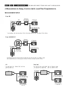
Page 4: ...s 250Hz 15kHz e g 7122 707 48001 LF Voltmeter e g PM2534 DUT S N and distortion meter e g Sound Technology ST1700B Frame aerial e g 7122 707 89001 Tuner AM MW LW To avoid atmospheric interference all AM measurements have to be carried out in a Faraday s cage Use a bandpass filter or at least a high pass filter with 250Hz to eliminate hum 50Hz 100Hz RF Generator e g PM5326 Ri 50Ω Bandpass 250Hz 15k...

Page 5: ...al Torx driver holder 4822 395 91019 Torx bit T10 150mm 4822 395 50456 Torx driver set T6 T20 4822 395 50145 Torx driver T10 extended 4822 395 50423 Compact Disc SBC426 426A Test disc 5 5A 4822 397 30096 SBC442 Audio Burn in Test disc 1kHz 4822 397 30155 SBC429 Audio Signals disc 4822 397 30184 Dolby Pro logic Test Disc 4822 395 10216 ...

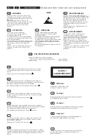
Page 6: ...la massa dell apparecchio tramite un braccialetto a resistenza Assicurarsi che i componenti e anche gli utensili con quali si lavora siano anche a questo potenziale GB ESD PROTECTION EQUIPMENT Complete Kit ESD3 small tablemat wristband connection box extention cable and earth cable 4822 310 10671 Wristband tester 4822 344 13999 CLASS 1 LASER PRODUCT GB Warning Invisible laser radiation when open A...

Page 7: ...void wear out of tips switch off un used equipment or reduce heat Mix of lead free solder alloy parts with leaded solder alloy parts is possible but PHILIPS recommends strongly to avoid mixed solder alloy types leaded and lead free If one cannot avoid or does not know whether product is lead free clean carefully the solder joint from old solder alloy and re solder with new solder alloy SAC305 Use ...

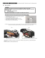
Page 8: ...t a paper clip on the flexfoil to short circuit the contacts fig 1 5 Replace the defective loader with a new loader 6 Remove paperclip from the flexfoil and connect it to the new loader 7 Remove solder joint on the ESD protection point ATTENTION The laser diode of this loader is protected against ESD by a solder joint which shortcircuits the laserdiode to ground For proper functionality of the loa...

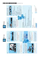
Page 9: ...TV C Place the front speakers at equal disctances from the TV D Place the rear speakers at normal listening ear level B Connect the radio antennas Keep the antennas away from the electronic devices to prevent unwanted interference A B C A Connect the FM antenna to the FM socket Extend the wire and fix its end to the wall B Unfold the AM MW loop antenna and fix the claw into the slot C Push the tab...

Page 10: ...s N V All rights reserved 12 NC 3139 245 23741 www philips com 2 Set up A Finding the viewing channel A Press STANDBY ON on the DVD system B Press SOURCE on the DVD system until DISC appears on the display panel C Turn on the TV Use the TV s remote control to select the correct viewing channel for the DVD system You should see the blue DVD background on the TV Note To search for the correct viewin...

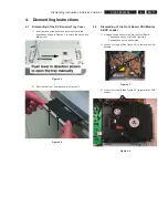
Page 11: ...e bottom side 2 Loosen 4 screws A See Figure 4 3 to remove the PSU Module Figure 4 3 3 Loosen 4 screws B See Figure 4 4 to remove the DVD Loader Figure 4 4 4 Dismantling Instructions 4 1 Dismantling of the DVD Loader Tray Cover 1 Insert a minus screwdriver and push the lever in the direction as shown in Figure 4 1 to unlock the tray before sliding it out Figure 4 1 2 Remove the Tray Cover as shown...

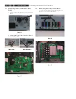
Page 12: ...ee Figure 4 5 to remove the Tuner Module Figure 4 5 2 Loosen 2 screws D and E See Figure 4 6 Figure 4 7 to remove the Mono Board Figure 4 6 AP Figure 4 6 Europe Figure 4 7 D C E F 4 4 Dismantling of the Amp module Board 1 Loosen 4 screws F and 2 screws G See Figure 4 8 Figure 4 9 to remove Amp Module Board Figure 4 8 Figure 4 9 G H H ...

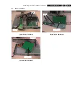
Page 13: ...antling Instructions Service Positions 4 5 Service Positions Service Position Front Board Service Position Amp Board Service Position Mono Board Insulation Sheet Amp Board Insulation Sheet Front Board Insulation Sheet Mono Board ...

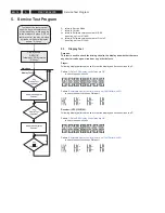
Page 14: ... display and whether there are any short circuits open circuits or any other defects Player Following display patterns are used to test the display and its connections to μP Pattern 1 Default All display control pins are ON to check the open circuits Pattern 2 Alternate display control pins are on Test Pattern 0x55 to check the short circuits on Data port Receiver HTS3100 3105 Following display pa...

Page 15: ...o the root directory of the new CD project 4 Burn the data onto a blank CDR or CDRW Note ISO9660 is mandatory UDF discs are not supported The final CDROM must not contain any other data except the file from the zip archive 5 1 4 Procedure to upgrade the firmware 1 Power up the set and open tray 2 Insert the prepared Upgrade CDROM and close the tray 3 The set will display LOAD Firmware Version UPG ...

Page 16: ...EN 16 3139 785 32300 5 Service Test Program Notes ...

Page 17: ...EN 17 3139 785 32300 6 Block Diagram Wiring Diagram Block Diagram MONO BD ERROR PSU 500 W Power Amplifier CONTROL HEF4052B Front Board 3139 249 38301 130 1 a2 pdf_2006_04_21 ...

Page 18: ... 3 4 5 1 10 9 2 2 3 2 1 2 VCC 6 4 12 3 1 11 0 1 4 2 1 14 13 9 7 8 VCC 9 16 9 4 5 1 1 8 2 3 2 1 6 12 2 1 TU_R 2 7 1 2 5 TU_L 8 7 7 8 1 2 8 1 TU_SD 9 8 7 6 5 1 3 1 2 3 4 7 0 7 1 1 0 5 1 2 1 7 1 3 3 1708 1 2 3 4 2 2 5 1 1 1 2 1 2 3 4 2 3 4 5 0 1 1 3 1 4 1 5 1 6 1 7 1 8 1 9 1 0 2 1 2 2 2 3 2 4 2 1 2 1 0 1 2 0 4 1 4 3 2 1 5 6 7 8 9 3 16 11 8 2 1 17 15 20 8 7 10 20 13 6 4 4 1 3 18 TU_L 9 8 7 6 5 4 3 2 1...

Page 19: ...4 G 5 8 F726 1701 HUV 08SS57T DSP 6 3 7 3 1 2 3 4 R 0 3 3 WH04D 1 1707 F724 MGND F718 6 1 3 S A B 8 0 7 6 F731 F729 5 2 7 3 K 0 1 8 1 7 2 n 0 0 1 p 0 0 1 4 3 7 2 2 6 1 7 3 3 K 3 7703 BC847B 1 3 BC847B 7708 2702 470n p 7 4 4 0 7 2 F725 F705 1 A 3 B 2 C 4 5 F704 EVEMC 1705 0 3 7 3 7 K 4 0 2 7 3 K 6 5 1 0 7 2 p 0 0 1 4 5 5 6 6 7 7 8 8 9 9 1 1 2 2 3 3 4 MGND MGND 1702 F728 10u 2724 6 1 3 S A B 0 u 1 7...

Page 20: ...EN 20 3139 785 32300 7 Front Display topview Circuit Diagram and PWB Layout HTS3115_DisplayTopView pdf_04_08_06 ...

Page 21: ...EN 21 3139 785 32300 Front Display Bottom view 7 Circuit Diagram and PWB Layout HTS3115_DisplayBottomView pdf_04_08_06 ...

Page 22: ...34 0 2 1 1 D R 0 D R 1 2 1 2 2 1 5 1 D R 4 1 D R 3 2 1 4 2 1 3 1 D R 2 1 D R 5 2 1 1 1 D R 6 2 1 7 2 1 0 1 D R 9 1 _ O I 3 1 1 7 D R 4 1 1 6 D R 5 1 1 5 D R 6 1 1 4 D R 3 D R 7 1 1 8 1 1 3 D D V D 2 D R 9 1 1 SA 12 6 0 1 5 _ 3 P U 7 0 1 E C I 8 0 1 T S R P R I 9 0 1 11 MD 0 1 1 0 T N I 0 M Q D 1 1 1 2 1 1 AGND 1 10 MC 5 _ 1 P U 0 0 1 1 0 1 6 _ 1 P U 2 0 1 7 _ 1 P U 3 0 1 0 _ 3 P U 1 _ 3 P U 4 0 1 ...

Page 23: ...239 3257 10K 2200 1u0 R 7 4 8 0 2 3 D 3 1 5 4 74LVC1G125GW 7200 2 3249 150R 2247 5211 BLM18P 100n 16V 47u 2244 150R 3252 3222 4R7 1 0 2 3 R 0 5 1 R 0 5 1 1 1 2 3 T204 4206 0 1 2 3 DV33 R 0 5 1 T211 T212 T206 3 3 V D 3251 150R T203 3261 150R 5 6 7 8 9 5212 BLM18P 14 15 16 17 18 19 2 20 3 4 1 10 11 12 13 20FE BT VK N 1201 2240 100n 9 0 2 2 p 7 4 5 0 2 2 p 7 4 T202 3264 150R 150R 3256 4 150R 3250 2 3...

Page 24: ... 47R R 3 3 2 4 3 3 R 0 3 3 5 2 3 3 3321 47R T305 2 3 3 3 K 0 1 5307 BLM18P DV33 T306 7 K 4 0 4 3 3 K 0 1 5 4 3 3 DV33 4 4 3 3 K 0 1 1302 R 3 3 9 2 3 3 200mA R 0 6 3 0 3 5 n 0 0 1 100n 2322 4 1 3 2 1 3 3 2 HDMI_3V3_A n 0 0 1 n 0 0 1 3 1 3 2 T307 V 6 1 u 0 1 HDMI_3V3_A R 0 6 5 1 0 3 3 7 2 3 2 0 4 2 S S V 19 VSSD 7 7 F R W 4 6 N D X VIE 0 8 F I V 13 VIG 1 VIH 9 7 F E R V 46 VSS1 1 51 VSS1 2 8 7 3 1 S...

Page 25: ... GND_tu GND_A GND_A 0 6 4 2 p 0 2 2 p 0 2 2 7 4 4 2 6 4 4 2 p 0 2 2 p 2 2 3 3 4 2 GND_A GND_A GND_A BC547B 2 3 1 3414 7403 D 1K5 2 K 2 7 1 4 3 p 2 8 2 1 4 2 F411 220K 3415 3410 2 6 4 3 K 0 2 2 1K0 GND_A GND_A GND_A GND_A T411 0 u 1 V 0 1 GND_tu K 7 4 5 3 4 2 GND_tu 0 6 4 3 4 2 4 3 K 0 0 1 7407 1 3 2 1 8 4 GND_A LM833D 2 0 4 4 GND_tu 6404 BZX384 C9V1 2400 100n 7 2 4 2 p 8 6 2429 1u0 4 13 6 3 11 GND...

Page 26: ...VL 6 K 5 GND_A D F501 F502 D 0 u 1 5 4 5 2 D F503 100p 2524 D p 0 0 1 5 2 5 2 2502 100p n 0 0 1 2 3 5 2 47K 3501 BC847B 470R 7500 D 3502 D 6 2 5 2 p 0 0 1 7504 BC807 25 F506 6 1 3 S A B 0 0 5 6 5VA D D GND_A 3 3 5 2 7502 PSS8550 u 0 0 1 3531 470R 12VA D 6 3 5 3 K 2 2 2 3 5 3 0 K 1 u 0 0 1 F509 9 2 5 2 1 3 5 2 V 6 1 u 7 4 F504 1 0 5 2 u 0 1 V 0 5 5 K 1 8 1 5 3 7503 3516 10R BC337 25 GND_A 12AM 12AM...

Page 27: ...EN 27 3139 785 32300 Layout Mono Board Top view 7 Circuit Diagram and PWB Layout HTS3115A_Analog_topwiftopview pdf_07_08_06 ...

Page 28: ...EN 28 3139 785 32300 Layout Mono Board Top Component with Bottom view 7 Circuit Diagram and PWB Layout HTS3115_Analog_topwifbtmview pdf_07_08_06 ...

Page 29: ...01 A2 1802 A1 2801 A1 1 2 1 2 A 3801 A2 6801 B2 F803 B F801 F802 6801 LTL 816EELC 470R 1 2 3 3801 B3B EH A 1802 2801 220p 1801 SKQNAB 3139 243 33842_StdbyBd_sh130_sh1 pdf_2005_11_16 StdbyBd_Topview_33842 pdf_022106 StdbyBd_Bottomview_33842 pdf_022106 Front Standby Top View Front Standby Bottom View ...

Page 30: ...EN 30 3139 785 32300 7 Circuit Diagram and PWB Layout PSU Circuit Diagram For information only PSU Europe AC8080SCH Europe_pg1 2 eps ...

Page 31: ...EN 31 3139 785 32300 7 Circuit Diagram and PWB Layout PSU Circuit Diagram For information only PSU Europe AC8080SCH Europe_pg2 2 eps ...

Page 32: ...EN 32 3139 785 32300 7 Circuit Diagram and PWB Layout PSU Circuit Diagram For information only PSU AP AC8082SCH AP_pg1 2 eps ...

Page 33: ...EN 33 3139 785 32300 7 Circuit Diagram and PWB Layout PSU Circuit Diagram For information only PSU AP AC8082SCH AP_pg2 2 eps ...

Page 34: ...OUT_D SD RESET_AB RESET_CD PVDD VGND OUT_B VDD 2 1 C14 100nF C14 100nF 1 2 R65 47R R65 47R 1 TP23 TP23 1 2 R79 10k R79 10k 1 TP32 TP32 1 3 2 Q41 PMBT2222 Q41 PMBT2222 1 2 R75 1 0k R75 1 0k 2 1 C25 100nF C25 100nF 1 2 R41 10k R41 10k 1 TP2 TP2 1 2 R70 10k R70 10k 1 2 R53 100k 0603 R53 100k 0603 2 1 C17 100nF C17 100nF 1 TP20 TP20 1 TP26 TP26 CHANNEL 1 4 Output Stage SE PWM_A PWM_B PWM_C PWM_D OUT_A...

Page 35: ... 220uF 35V 1 2 R114 100k 0603 R114 100k 0603 1 2 C163 220uF 35V C163 220uF 35V 1 2 L170 L170 2 1 C108 33nF 1206 100V C108 33nF 1206 100V 2 1 3 Q103 MMBT2907A Q103 MMBT2907A 1 2 R110 10R 0603 R110 10R 0603 1 2 R116 100k 0603 R116 100k 0603 2 1 C117 100nF 0805 50V C117 100nF 0805 50V 1 2 L173 L173 1 2 C162 220uF 35V C162 220uF 35V 2 1 C148 47nF 50V 0603 C148 47nF 50V 0603 1 2 R140 470R 0805 R140 470...

Page 36: ... 5 PWM_A 6 RESET_AB 7 PWM_B 8 OC_ADJ 9 GND 10 AGND 11 VREG 12 M3 13 M2 14 M1 15 PWM_C 16 RESET_CD 17 PWM_D 18 GVDD_C 22 GVDD_D 23 BST_D 24 PVDD_D 27 OUT_D 28 GND_D 29 GND_C 30 OUT_C 31 PVDD_C 32 BST_C 33 BST_B 34 PVDD_B 35 OUT_B 36 GND_B 37 GND_A 38 VDD 21 GVDD_A 44 BST_A 43 PVDD_A 40 OUT_A 39 NC 3 NC 4 NC 19 NC 20 NC 25 PVDD_D 26 PVDD_A 41 NC 42 U200 TAS5142DDV U200 TAS5142DDV 1 2 C274 220uF C274...

Page 37: ...R950 3 3R 0603 R950 3 3R 0603 1 TP41 TP41 2 1 C953 10nF 0603 50V C953 10nF 0603 50V 2 1 C951 10nF 0603 50V C951 10nF 0603 50V IN 1 GND 2 EN 3 BYPASS 4 OUT 5 U900 TPS76933 U900 TPS76933 2 1 C954 100nF 0805 50V C954 100nF 0805 50V 2 1 C950 100nF 0805 50V C950 100nF 0805 50V 1 2 3 4 5 6 7 8 J901 Header J901 Header 2 1 C905 100nF 0805 50V C905 100nF 0805 50V 1 2 R952 3 3R 0603 R952 3 3R 0603 1 2 C900 ...

Page 38: ...EN 38 3139 785 32300 8 Overview Modulator Input Output and Headphone Line Output Connectors Amp Board Layout Topview A785 PCB 002 2 00 _pg4 5 pdf ...

Page 39: ...EN 39 3139 785 32300 8 Overview Modulator Input Output and Headphone Line Output Connectors Amp Board Layout Bottomview ...

Page 40: ...EN 40 3139 785 32300 8 Overview Modulator Input Output and Headphone Line Output Connectors Notes ...

Page 41: ...EN 41 3139 785 32300 9 Exploded View of the Set Figure 9 1 9 Exploded View Spare Parts List ...

Page 42: ...MP 05 02 500W 1060 3139 248 50291 PCBAS FRONT HTS3115 EU 1080 2822 031 00048 FAN 12VDC 0 5W 3700RPM B 1090 3139 248 50301 PCBAS MONO HTS3115 EU 1101 3139 241 00341 FFC FOIL 24P 220 24P AD 0 5MMP 8001 3139 241 01381 FFC FOIL10P 120 10P AD FOLD 8005 3139 241 02011 FFC FOIL 20P 140 20P AD SPK ASSY SW 3110 9965 000 35004 SW3105 SUBWOOFER BOX 9965 000 34997 RUBBER FOOT SW 9965 000 34998 CABLE A SSY 5 3...

Reviews: