LS
HS
LS
HS
OSC/RAMP
MUTE
CONTROL
BYPASS
AV
CONTROL
CONTROL
BIAS
THERMAL
SC
DETECT
SC
DETECT
AVDD
AVCC
LIN
RIN
MUTE
BYPASS
GAIN1
GA N0
SD
BSL
PVCCL
LOUT
PGNDL
VCLAMP
BSR
PVCCR
ROUT
PGNDR
VCLAMP
VCLAMP
AVDD
AVDD
AVDD/2
AVDD
AVDD
AVDD/2
REGULATOR
AGND
+
-
+
-
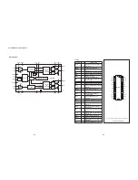
TPA3123D2 BLOCK DIAGRAM
U1,U3 -- TPA3123D2 IC Specification
Table 1. TERMINAL FUNCTIONS
TERMINAL
I/O/P
DESCRIPTION
24-PIN
NAME
(PWP)
Shutdown signal for IC (low = disabled, high = operational). TTL logic levels with compliance to
SD
2
I
AVCC
RIN
6
I
Audio input for right channel
LIN
5
I
Audio input for left channel
GAIN0
18
I
Gain select least-significant bit. TTL logic levels with compliance to AVCC
GAIN1
17
I
Gain select most-significant bit. TTL logic levels with compliance to AVCC
Mute signal for quick disable/enable of outputs (high = outputs switch at 50% duty cycle, low =
MUTE
4
I
outputs enabled). TTL logic levels with compliance to AVCC
BSL
21
I/O
Bootstrap I/O for left channel
PVCCL
1, 3
P
Power supply for left-channel H-bridge, not internally connected to PVCCR or AVCC
LOUT
22
O
Class-D 1/2-H-bridge positive output for left channel
PGNDL
23, 24
P
Power ground for left-channel H-bridge
VCLAMP
11
P
Internally generated voltage supply for bootstrap capacitors
BSR
16
I/O
Bootstrap I/O for right channel
ROUT
15
O
Class-D 1/2-H-bridge negative output for right channel
PGNDR
13, 14
P
Power ground for right-channel H-bridge.
PVCCR
10, 12
P
Power supply for right-channel H-bridge, not connected to PVCCL or AVCC
AGND
9
P
Analog ground for digital/analog cells in core
AGND
8
P
Analog ground for analog cells in core
Reference for preamplifier inputs. Nominally equal to AVCC/8. Also controls start-up time via
BYPASS
7
O
external capacitor sizing.
AVCC
19, 20
P
High-voltage analog power supply. Not internally connected to PVCCR or PVCCL
Connect to ground. Thermal pad should be soldered down on all applications to properly
Thermal pad
Die pad
P
secure device to printed wiring board.
1
2
3
4
5
6
7
8
9
10
11
12
24
23
22
21
20
19
18
17
16
15
14
13
PVCCL
SD
PVCCL
MUTE
LIN
RIN
BYPASS
AGND
AGND
PVCCR
VCLAMP
PVCCR
PGNDL
PGNDL
LOUT
BSL
AVCC
AVCC
GAIN0
GAIN1
BSR
ROUT
PGNDR
PGNDR
PWP (TSSOP) PACKAGE
(TOP VIEW)
17-3
17-3
Summary of Contents for HTS3220
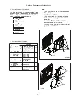
Page 21: ...9 2 Fig D3 Fig D4 Fig D5 Cabinet Disassembly Instructions A10 A09 A09 A02 A02 A03 A03 ...
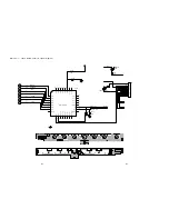
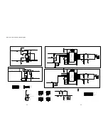
Page 30: ...Main Unit VFD Display Board Layout Diagram 15 3 15 3 ...
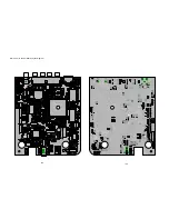
Page 35: ...Main Unit AMP Board Layout Diagram 17 4 17 4 ...
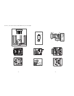
Page 44: ...Main Unit Decoder Board Layout Diagram 18 9 18 9 ...
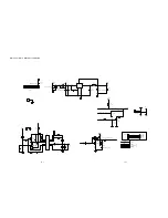
Page 45: ...Subwoofer AMP Power Board Circuit Diagram 19 1 19 1 ...
Page 46: ...Subwoofer AMP Power Board Circuit Diagram 19 2 19 2 IC5 TDA8920CJ ...
Page 48: ...Subwoofer AMP Power Board Layout Diagram 19 4 19 4 ...
Page 49: ...Main Unit Exploded View 20 1 20 1 ...
Page 50: ...Subwoofer Exploded View 20 2 20 2 SUB016 For 98version ...
Page 52: ...Revision List Revision List Version 1 0 Initial Release 21 1 ...

