18-4
18-4
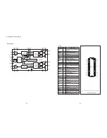
U11: EN29LV320A IC Specification
PRODUCT SELECTOR GUIDE
A
0
2
3
V
L
9
2
N
E
r
e
b
m
u
N
t
c
u
d
o
r
P
Speed Option
-70
-90
Max Access Time, ns (t
acc
B
)
70
90
Max CE# Access, ns (t
ce
B
)
70
90
Max OE# Access, ns (t
oe
B
)
30
35
Notes:
1. Vcc=3.0 – 3.6 V for 70ns read operation
BLOCK DIAGRAM
WE#
CE#
OE#
State
Control
Command
Register
Erase Voltage Generator
Input/Output Buffers
Program Voltage
Generator
Chip Enable
Output Enable
Logic
Data Latch
Y-Decoder
X-Decoder
Y-Gating
Cell Matrix
Timer
Vcc Detector
A0-A20
Vcc
Vss
DQ0-DQ15 (A-1)
Ad
dre
ss
La
tch
Block Protect Switches
STB
STB
RY/BY#
32M FLASH USER MODE TABLE
DQ8-DQ15
Operation
CE#
OE#
WE#
RESET
#
WP#/AC
C
A0-
A20
DQ0-
DQ7
BYTE#
= V
B
IH
B
BYTE#
= V
B
IL
B
Read
L
L
H
H
L/H
A
B
IN
B
D
OUT
B
D
OUT
B
Write
L
H
L
H
(Note 1)
A
B
IN
B
D
B
IN
B
D
B
IN
B
Accelerated
Program
L
H
L
H
V
HH
A
B
IN
B
D
B
IN
B
D
B
IN
B
DQ8-
DQ14=
High-Z,
DQ15 =
A
-1
CMOS Standby
V
cc
B
±
0.3V
X
X
V
cc
B
±
0.3V
H
X
High-Z
High-Z
High-Z
TTL Standby
H
X
X
H
H
X
High-Z
High-Z
High-Z
Output Disable
L
H
H
H
L/H
X
High-Z
High-Z
High-Z
Hardware Reset X
X
X
L
L/H
X
High-Z
High-Z
High-Z
Sector (Group)
Protect
L
H
L
V
B
ID
B
L/H
SA,
A6=L,
A1=H,
A0=L
(Note 2) X
X
Sector
Unprotect
L
H
L
V
B
ID
B
(Note 1)
SA,
A6=H,
A1=H,
A0=L
(Note 2) X
X
Temporary
Sector
Unprotect
X
X
X
V
B
ID
B
(Note 1)
A
B
IN
B
(Note 2)
(Note 2)
High-Z
L=logic low= V
B
IL
B
, H=Logic High= V
B
IH
B
, V
B
D
B
=V
HH
=11 ± 0.5V = 10.5-11.5V, X=Don’t Care (either L or H, but not floating ),
SA=Sector Addresses, D
B
IN
B
=Data In, D
OUT
B
=Data Out, A
B
IN
B
=Address In
Notes:
1. If WP#/ACC =
V
IL
B
, the two outermost boot sectors remain protected. If WP# / ACC =
V
IH
B
, the outermost boot sector
protection depends on whether they were last protected or unprotected. If WP#/ACC =
V
HH
B
, all sectors will be
unprotected.
2. Please refer to “Sector/Sector Group Protection & Chip Unprotection”, Flowchart 7a and Flowchart 7b.
Summary of Contents for HTS3220
Page 21: ...9 2 Fig D3 Fig D4 Fig D5 Cabinet Disassembly Instructions A10 A09 A09 A02 A02 A03 A03 ...
Page 30: ...Main Unit VFD Display Board Layout Diagram 15 3 15 3 ...
Page 35: ...Main Unit AMP Board Layout Diagram 17 4 17 4 ...
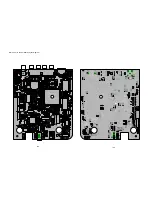
Page 44: ...Main Unit Decoder Board Layout Diagram 18 9 18 9 ...
Page 45: ...Subwoofer AMP Power Board Circuit Diagram 19 1 19 1 ...
Page 46: ...Subwoofer AMP Power Board Circuit Diagram 19 2 19 2 IC5 TDA8920CJ ...
Page 48: ...Subwoofer AMP Power Board Layout Diagram 19 4 19 4 ...
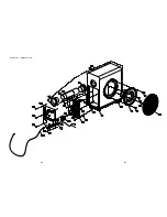
Page 49: ...Main Unit Exploded View 20 1 20 1 ...
Page 50: ...Subwoofer Exploded View 20 2 20 2 SUB016 For 98version ...
Page 52: ...Revision List Revision List Version 1 0 Initial Release 21 1 ...


