background image

Published by KC-TE 0519 AV Systems   

Printed in  he Netherlands  

Subject to modifi cation  

EN 3139 785 31180

HTS5000W

/

51/12

DVD Receiver

CLASS  1

LASER PRODUCT

1 Technical 

Specifi cations and Connection

 Facilities 

2

Measurements Setup, Service Aid & 


Lead Free Requirements  

4

Directions For Use 

8

Dismantling Instructions & Service Positions 

10

Service Test Program  

13

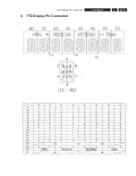
FTD Display Pin Connection 

15

7 Block 

Diagram 

17

 Wiring 

Diagram 

18

Circuit Diagram and PWB Layout 

19 


 Front: 

Display 

19  


Front: Display (Top view) 

20 


Front: Display (Bottom view) 

21 


Mono Board: Circuit Diagram (Part 1) 

22


Mono Board: Circuit Diagram (Part 2) 

23


Mono Board: Circuit Diagram (Part 3) 

24


Mono Board: Circuit Diagram (Part 4) 

25


Mono Board: Circuit Diagram (Part 5) 

26


Mono Board: Circuit Diagram (Part 6) 

27


Mono Board: Circuit Diagram (Part 7) 

28


Mono Board: Circuit Diagram (Part 8) 

29


Mono Board: Circuit Diagram (Part 9) 

30


Layout: Mono Board (Top View) 

31


Layout: Mono Board (Bottom View) 

32


Standby Board: Circuit Diagram 

33


Layout: Standby Board (Topview) 

34

©Copyright 2005 Philips Consumer Electronics B.V. Eindhoven, The Netherlands.
All rights reserved. No part of this publication may be reproduced, stored in 
a retrieval system or transmitted, in any form or by any means, electronic, 
mechanical, photocopying, or otherwise without the prior permission of Philips.

Version 1.0

Contents Page

Contents Page


Layout: Standby Board (Bottom view) 

35


USB Board: Circuit Diagram 

36


Layout: USB Board (Topview) 

37


Layout: USB Board (Bottom view) 

38


PSU Circuit Diagram (For information only) 

39

Exploded View & 


Module PWR 04-01 Non-Wireless 

41 


Exploded View of the set 

41 


Module PWR 04-01 Non-Wireless 

42


Overview - introduction 

42

 Electrical 

specifi cation 

42

 Key 

components 

42


Introduction & defi nitions 

43

 Overview 

of 

Testpoints 

44


Test Setup and start up 

44

 DC 

MEASUREMENTS 

45

 AUDIO 

MEASUREMENTS 

48

 Connections 

50

 Block 

diagram 

51

 Mute 

circuitry 

52

 Amplifi er considerations 

53


Volume chip M62429FP 

54


Module PWR 04-01 Non-Wireless:  


Circuit Diagram (Part 1) 

55


Module PWR 04-01 Non-Wireless:  


Circuit Diagram (Part 2) 

56


Module PWR 04-01 Non-Wireless:  


Circuit Diagram (Part 3) 

57


Layout: Module PWR 04-01  


 Non-Wireless 

(Topview) 

58


Layout: Module PWR 04-01  


Non-Wireless (Bottom view) 

59

10 Spare Parts List 

61

Summary of Contents for HTS5000W/12

Page 1: ...opyright 2005 Philips Consumer Electronics B V Eindhoven The Netherlands All rights reserved No part of this publication may be reproduced stored in a retrieval system or transmitted in any form or by any means electronic mechanical photocopying or otherwise without the prior permission of Philips Version 1 0 Contents Page Contents Page Layout Standby Board Bottom view 35 USB Board Circuit Diagram...

Page 2: ...ations and Connection Facilities VERSION VARIATIONS HTS5000W 12 HTS5000W 51 Video Yellow Cinch x x Component Video Y Pb Pr P scan x x SCART CVBS RGB x Digital In Coaxial x x TV In Left Right x Auxiliary Left Right x x Line out Audio x x ...

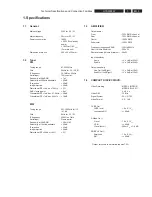
Page 3: ...y 450kHz 1kHz Aerial input Frame aerial Sensitivity at 26dB S N 4 0mV M Selectivity at 18kHz bandwidth 20dB IF rejection 45dB Image rejection 28dB Distortion at RF 50mV m 80 5 1 3 AMPLIFIER Output power Front 75W RMS channel Rear 75W RMS channel Center 100W RMS Subwoofer 100W RMS Frequency response 0 5dB 120Hz 20kHz Hum Volume Minimum 200nW Residual noise Volume Minimum 40nW Input sensitivity Aux ...

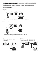
Page 4: ...50Hz 15kHz e g 7122 707 48001 LF Voltmeter e g PM2534 DUT S N and distortion meter e g Sound Technology ST1700B Frame aerial e g 7122 707 89001 Tuner AM MW LW To avoid atmospheric interference all AM measurements have to be carried out in a Faraday s cage Use a bandpass filter or at least a high pass filter with 250Hz to eliminate hum 50Hz 100Hz RF Generator e g PM5326 Ri 50Ω Bandpass 250Hz 15kHz ...

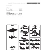
Page 5: ...Torx driver holder 4822 395 91019 Torx bit T10 150mm 4822 395 50456 Torx driver set T6 T20 4822 395 50145 Torx driver T10 extended 4822 395 50423 Compact Disc SBC426 426A Test disc 5 5A 4822 397 30096 SBC442 Audio Burn in Test disc 1kHz 4822 397 30155 SBC429 Audio Signals disc 4822 397 30184 Dolby Pro logic Test Disc 4822 395 10216 ...

Page 6: ...massa dell apparecchio tramite un braccialetto a resistenza Assicurarsi che i componenti e anche gli utensili con quali si lavora siano anche a questo potenziale GB ESD PROTECTION EQUIPMENT Complete Kit ESD3 small tablemat wristband connection box extention cable and earth cable 4822 310 10671 Wristband tester 4822 344 13999 CLASS 1 LASER PRODUCT GB Warning Invisible laser radiation when open Avoi...

Page 7: ...d wear out of tips switch off un used equipment or reduce heat Mix of lead free solder alloy parts with leaded solder alloy parts is possible but PHILIPS recommends strongly to avoid mixed solder alloy types leaded and lead free If one cannot avoid or does not know whether product is lead free clean carefully the solder joint from old solder alloy and re solder with new solder alloy SAC305 Use onl...

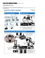
Page 8: ...b Pr Y WIRELESS REAR SPEAKER ANTENNA FRONT L FRONT R CENTRE REAR L REAR R Note For connecting to a Progressive ScanTV refer to the user manual for proper connections and detailed set up A E 3d Connect the FM and MW antennas 3b Connect the front speakers and subwoofer to the DVD system refer to the user manual for Individual speaker volume adjustment FRONT R Subwoofer REAR L REAR R FRONT L CENTRE T...

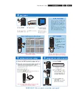
Page 9: ...in the user manual for detailed descriptions 1 2 More settings and features GET SOUND To enhance the sound quality Press SOUND button to select a predefined digital sound effect Detailed playback features and additional functions are described in the user manual No sound from rear speakers Press SURR button to select Multi Channel 5 wireless receiver setup 6 programme radio stations NEEDS HELP Vis...

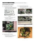
Page 10: ...SU Board 1 The disc can be manually remove by inserting a minus screw driver and push the lever in the direction as shown in Figure 3 1 to unlock the tray and eject the disc out Figure 4 1 2 Loosen 5 screws Pos 272 to remove the Front Top 1 screw each on the left and right side 3 screws at the rear of the set 3 Loosen 4 screws Pos 258 to remove PSU Board as shown in Figure 3 2 Figure 4 2 4 2 Disma...

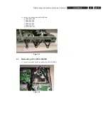
Page 11: ...ns 4 4 Loosen 8 screws to remove Mono Board 2 screws Pos 262 1 screw Pos 265 1 screw Pos 268 1 screw Pos 264 1 screw Pos 267 2 screws Pos 269 Figure 4 7 4 4 Dismantling of the DVD LOADER 1 Loosen 4 screws Pos 254 to remove the DVD LOADER Figure 4 8 F F F G ...

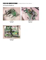
Page 12: ... Service Positions 4 5 Service Positions Figure 4 9 Service Position PSU Board Figure 4 11 Service Position Front Panel Figure 4 10 Service Position Mono Board PSU Board Mono Board Front Panel Insulation Sheet Insulation Sheet Insulation Sheet ...

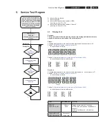
Page 13: ...umber of Front uP counting up from 01 to 99 4 1 Display Test Purpose This test is used to check the driving circuits the display and whether there are any short circuits open circuits or any other defects Player Following display patterns are used to test the display and its connections to μP Pattern 1 Default All display control pins are ON to check the open circuits Pattern 2 Alternate display c...

Page 14: ...ve into the root directory of the new CD project 4 Burn the data onto a blank CDR or CDRW Note ISO9660 is mandatory UDF discs are not supported The final CDROM must not contain any other data except the file from the zip archive 5 1 4 Procedure to upgrade the firmware 1 Power up the set and open tray 2 Insert the prepared Upgrade CDROM and close the tray 3 The set will display LOAD MULTICH UPG END...

Page 15: ...EN 15 HTS5000W FTD Display Pin Connection 6 6 FTD Display Pin Connection ...

Page 16: ...EN 16 HTS5000W Notes 6 FTD Display Pin Connection ...

Page 17: ...CK 22 TRACK 23 FOC 24 FOC 1101 GND_LD 1 DVD LD 2 NC 3 HFM 4 MD 5 CD_LD 6 VD_DVD 7 VD_CD 8 NC 9 E 10 VCC 11 VREF 12 GND 13 F 14 B 15 A 16 RF 17 CD_DVD SW 18 C 19 D 20 TRACK 21 TRACK 22 FOC 23 FOC 24 7203 M29W160ET70 FLASH 5M L_V33 L_V33 7110 MM1646XH Motor Drivers LOAD 1 LOAD 2 TROUT 3 GND 4 TRIN 5 1105 7200 IM24C16 RDW6 NVRAM 1109 1401 5130 27MHZ 7202 CS8415A Digital Audio Interface receiver 1502 ...

Page 18: ...313911101901 MIS 09 340 09 OE 5VL 12VL GND 5V EV 24V VSTB VSTA VSCK GND 41K RC6 STBY NC NC 1 9 1 5 9P EH BOARD INTO MONO Front MIC 3139 113 35771 3139 113 35761 FR1 2 layer 2P stand by switch 313911104521 MIS 04 480 04 OE 8701 313911103311 MIS 02 220 02 OE 313911103541 MIS 05 18 3139 243 31471 141X382 FR4 2 layer 12VA MIC GND 12A 4P EH TO mono MIC Port s TU_SCL TU_SDA TU_SD TU_L TU_Stereo TU_R NC ...

Page 19: ... 9 1 2 3 4 28 29 30 31 32 35 15 36 16 17 18 50 49 48 47 46 52 24 25 26 27 42 41 40 39 38 37 7 10 11 12 13 8 6 5 44 43 n 0 0 1 7708 UPD16311GC AB6 Φ FIP CONTROLLER DRIVER 6 1 7 2 4 1 7 2 p 0 1 10u 2724 0 2 7 2 p 0 0 1 6 0 7 2 0 u 1 4 P 6 2 5 P 5 2 6 P 4 2 7 P 3 2 8 P 2 2 9 P 1 2 F729 8 1 2 1 P 3 1 P 7 1 6 1 4 1 P 5 1 5 1 P 4 1 6 1 P 7 1 P 3 1 8 2 2 P 3 P 7 2 G 6 9 G 7 0 1 G 8 1 1 1 F 1 2 F 2 3 1 P ...

Page 20: ...EN 20 HTS5000W 8 Front Display topview FrontBoard_TopView_3139_113_35766 pdf_090205 Circuit Diagram and PWB Layout ...

Page 21: ...EN 21 HTS5000W Front Display Bottom view FrontBoard_BottomView_3139_113_35766 pdf_090205 8 Circuit Diagram and PWB Layout ...

Page 22: ...C A A S S V C A D 1 0 2 2 0 2 5 V U Y 6 V U Y 3 0 2 4 0 2 9 _ 3 D D V D 5 0 2 N Y S V 6 0 2 7 V U Y 7 0 2 N Y S H 8 0 2 K L C M P S 5 9 1 B D D V C A D 6 9 1 2 V U Y 7 9 1 B S S V C A D 3 V U Y 8 9 1 9 9 1 A D D V C A D 2 DVDA MDI1 20 4 V U Y 0 0 2 RD16 189 DACVDDC TPI 19 190 VREF FS 191 192 YUV0 C S S V C A D 3 9 1 1 V U Y 4 9 1 180 181 RD22 DVDD3 8 182 183 RD21 184 RD20 185 RD19 186 RD18 187 RD1...

Page 23: ...29W160ET70 25 24 6 5 4 3210 3 3 6 10R 2269 100n 10R 1 8 D 3211 1 3214 4 4 5 10R 2257 100n D 2258 47u 16V 8 3235 22R 3214 1 10R 1 2 7 10R 3210 2 T237 4201 3202 10K 3241 33R 3212 4 10R 4 5 4 3 2 3 R 0 7 2 10R 3211 2 2 7 10K 3240 D p 2 2 9 5 2 2 3211 3 3 6 D 10R n 7 4 3 7 2 2 3227 D 22R 5200 2254 100n 3231 1 8 22R 3213 1 10R 2 6 2 2 p 2 2 100n 2252 2256 3200 10K 100n 100n 2268 10K 3201 D 4 5 6 2 1 6 ...

Page 24: ...6 6304 T304 T303 3321 100K T310 T309 3320 6K8 T314 4301 3327 47K 47K 5 4 1 7 6 3326 F305 7302 3 74HCU04D 602K7 1300 3304 5K6 0 4 3 3 0 K 1 BC847B 7308 1 3 2 3343 4K7 V 6 1 u 2 2 6 2 3 2 74HCU04D 1 4 1 7 2 7302 1 2308 100n 5300 0 K 1 2 2 3 3 p 0 0 1 6 0 3 2 4 0 1 3 3 7302 2 3 4 1 7 3323 74HCU04D 1M0 BC847B 7300 74HCU04D 11 4 1 7 10 7302 5 5 2 3 2 n 0 0 1 K 0 1 100n 2304 1 3 3 3 5 0 3 2 u 0 1 6306 B...

Page 25: ...20 STABI MODE OSC STAGE STAGE INP INP MANAGER PWM PWM MOD MOD CURRENT PROT TEMP SENSOR CTRL CTRL SHAKE SHAKE HAND HAND DRIVER DRIVER DRIVER DRIVER HIGH HIGH LOW LOW 9 0 4 T 2429 100n 1 2 22u 5402 100n 2430 F407 2411 220p 9 1 4 3 R 0 1 1 1 4 T R 0 1 0 1 4 3 2405 100n 2 1 4 T 5 1 4 T 6 1 4 T T405 0 1 4 T 100n 2452 100n 2428 100n 2406 2 1 4 3 4 3 4 2 K 7 4 p 0 3 3 2425 100n 2431 100n p 0 2 2 2427 0 2...

Page 26: ...16 12AM 7504 1 GND_A F507 6 2 5 3 GND_A K 2 2 F513 GND_A 3 2 1 4 8 GND_A 7500 1 LM833D 8 K 6 7 4 5 3 3534 4K7 7 0 5 2 p 8 6 5K6 2 2 3 3 4 4 5 5 6 6 7 7 8 8 9 9 3527 1 1 10 1K2 3521 1 1 5 2 3507 10K p 0 0 1 3500 10K 7502 GND_A 8 1 5 2 BC547B p 8 6 4507 GND_A GND_A GND_A 4517 8 2 5 3 8 K 6 4515 F505 2506 1u0 3529 4K7 10K 3502 3 1 2 LPR6520 J920G 1501 GND A K 2 2 GND_A F523 2 2 5 3 F511 GND_A GND_A G...

Page 27: ...7 4K7 GND A 9 1 6 2 0 u 1 GND_A 2u2 2610 2620 10u 25V 10K 3660 2K2 3663 p 0 2 2 7 8 6 2 p 7 4 A V 5 GND A 9 8 6 2 D 4 7 6 2 n 0 0 1 GND A 2u2 5605 3630 12K 2K2 2 4 6 2 D 3635 T607 p 7 4 T606 12K 3644 GND A 2614 100n 2695 100n T602 T603 3V3_D 12AM 0 4 6 2 p 0 2 2 2K2 3645 p 0 2 2 2 6 6 2 p 7 4 4 6 6 2 D 5K1 3647 D GND_A 4601 GND_A 3K3 D 12AM DAC_C 3664 2681 2u2 D A _ 3 V 3 3648 4K7 33R 3612 GND A 1...

Page 28: ...708 T709 3V3 100n 2732 3704 3788 3K3 7714 4K7 BC847B BAS316 6718 BAS316 6725 2733 47u 16V 4 12AM GND A LM833D 7711 2 5 6 7 8 3705 1u0 4K7 2716 K 7 4 220K 3781 GND A 8 5 7 3 3V3 GND A BAS316 6720 6723 BAS316 1u0 2712 K 7 4 7 6 7 3 BAS316 6716 680R 3762 6 K 5 4 7 7 3 6719 BAS316 GND A GND A 4 3793 470R BC847BPN 7724 2 5 3 6 6 7 3 K 7 4 T256 T714 3787 4K7 12AM 2721 5K1 3722 56p 470R 3785 16V 100u 271...

Page 29: ...2 6 4 4 5 6 7 8 9 14 15 16 17 18 19 2 20 21 3 1800 1 10 11 12 13 035 0 9848 00 T806 T805 R 2 8 3833 BC847BPN 2 6 1 D 5V 7804 1 T803 R 0 2 2 1 4 8 3 n 2 2 9 1 8 2 3820 10K D 2 4 8 3 R 0 2 2 T804 T817 5V D 12VL K 2 2 8 5 8 3 4807 T816 F804 3 4 8 3 R 0 2 2 D 2 u 2 2850 T809 D 1802 C MSP 801V1 02 01 B NI FE LF GND 8 5V 2818 T812 220p 2815 220p D 4 5 D 1802 A MSP 801V1 02 01 B NI FE LF 1 2 3 6 D 5V D M...

Page 30: ...1 A2 T902 B2 T903 A5 B 1901 1 2 F913 2 0 9 3 B2B EH A 6 R 5 5 K 1 7 0 9 3 R 0 7 4 3 0 9 3 T902 T903 T900 T901 D GND_A 3V3 D D 5VL F901 12A 12A 3V3 D D n 0 1 0 2 9 2 F906 8 1 9 2 p 0 0 1 2914 10n F903 F910 F909 10n 2913 n 0 1 2 1 9 2 D 3V3 10n 2911 7900 n 0 1 BC327 25 BZX384 C4V7 2 0 9 2 4 5 6 7 8 9 6900 1900 B12B EH A 1 10 11 12 2 3 R 8 6 8 0 9 3 u 0 1 0 0 9 2 1 3 2 D 7901 LD1117DT F902 R 0 2 1 5 ...

Page 31: ...EN 31 HTS5000W Layout Mono Board Topview Circuit Diagram and PWB Layout MonoBoard_TopView_3139_113_36003 pdf_090205 8 ...

Page 32: ...EN 32 HTS5000W Layout Mono Board Bottom view Circuit Diagram and PWB Layout MonoBoard_BottomView_3139_113_36003 pdf_090205 8 ...

Page 33: ...rcuit Diagram 1901 A1 1 2 1 2 A B A B 1900 A1 F901 A1 2901 B1 2902 B1 F902 A1 p 0 2 2 1 0 9 2 SKQNAB 1901 1 2 B2B EH A 1900 F902 F901 p 0 2 2 2 0 9 2 Circuit Diagram and PWB Layout StandbyBoard_3139_113_35776_a4_sh130_1 pdf_051805 8 ...

Page 34: ...EN 34 HTS5000W Layout Standby Board Topview Circuit Diagram and PWB Layout StandbyBoard_TopView_3139_113_35776 pdf_090205 8 ...

Page 35: ...EN 35 HTS5000W Layout Standby Board Bottom view StandbyBoard_BottomView_3139_113_35776 pdf_090205 Circuit Diagram and PWB Layout 8 ...

Page 36: ...2803 B2 3801 A1 3802 A1 3803 A1 F801 A2 F802 A2 F803 A2 F804 A2 1 1 p 2 2 3 0 8 2 22R 3802 F801 3 4 5 6 F802 5401 042 101 92 1800 1 2 p 2 2 2 0 8 2 2 3 4 p 2 2 1 0 8 2 1801 WH04D 1 1 3803 3801 22R F804 F803 USB_Board_3139_113_35986_a4_sh130_1 pdf_051805 Circuit Diagram and PWB Layout 8 ...

Page 37: ...EN 37 HTS5000W Layout USB Board Topview USB_Board_TopView_3139_113_35986 pdf_090205 Circuit Diagram and PWB Layout 8 ...

Page 38: ...EN 38 HTS5000W Layout USB Board Bottom view USB_Board_BottomView_3139_113_35986 pdf_090205 Circuit Diagram and PWB Layout 8 ...

Page 39: ...EN 39 HTS5000W PSU Circuit Diagram For information only 5 0 0 2 5 0 _ f d p 1 0 1 1 4 0 2 0 7 1 m a r g a i D t i u c r i C 1 0 4 0 U S P Circuit Diagram and PWB Layout 8 ...

Page 40: ...EN 40 HTS5000W Notes Circuit Diagram and PWB Layout 8 ...

Page 41: ...EN 41 HTS5000W 9 Exploded View of the Set Figure 8 1 9 Exploded View Module PWR 04 01 Non Wireless HTS3500S 12_3139 249 2690_051305 ...

Page 42: ...ut for 50Watt into 6 ohm see annex 1 FTC power THD 0 1 at 1 8 P rated each channel separately measured Frequency response flat between 30Hz 20kHz 1 dB Phase Input and output in phase Typical DC supply 27 VDC 27 VDC 6VDC Load output 6 ohm Both channels should be loaded with 6 ohms to avoid audioholes Mute input Active low Standby input Active low Leds Green playmode or muted red is standbymode Stan...

Page 43: ... developed tool to give the correct serial data to the volumechip otherwise no testing is possible testtool 3104 137 00231 Also before connecting the amplifier to the power supply and applying inputsignals be sure that the heatsink is mounted in all other cases excessive temp rise and thermal shutdown of the TDA8920TH is possible See below picture schematic to have an idea how the final receiverse...

Page 44: ...used to control the serial data and clock towards the volumechip via DB9 serial cable towards any IBM PC DTR clock pin 4 of DB9 RTS DATA pin 7 of DB9 This testtool has on board loads 50 ohms for the 6Vdc and 100 ohms for the 3 3Vdc Two cinch connectors are forseen to connect an audiosource with Zout 600ohms Mute and standby can be simulated on this testboard with switches or with relay s to an aut...

Page 45: ...artup startup amp muted and or standby Be sure the heatsink is mounted in the correct way 7 DC MEASUREMENTS Pcb connected to the testtool all supplies connected as described above No audioinput signals to the PCB F1 an F3 to ground Audio inputs F10 standby F11 mute DVD F16 mute RX low at startup by use of the switches on the tool Static DC measurements all values Vdc F32 5Vdc F35 15Vdc F36 15Vdc F...

Page 46: ...muted 2 5 3 2 0 1 0 1 4 5 0 1 3 1 Typical 2 2 2 9 0 0 3 8 Lower 2 7 3 5 0 3 0 3 4 7 Higher F16 to 3 3Vdc F10 F11 to 3 3Vdc Amp on demuted playmode 5 0 1 0 1 0 1 4 5 0 1 3 1 Typical 4 6 0 0 0 3 8 Lower 5 3 0 3 0 3 0 3 4 7 Higher Condition Amplifier in Play mode Action Switch off the 27v dc supply and check the levels on F39 MODE_AMP 2 5 Typical 2 2 Lower 2 7 Higher Condition Amplifier powered Actio...

Page 47: ...ical 80 75 170 Lower 100 95 175 Higher Dynamic DC measurements Serial communication all values Vdc The below table is valid if the 5Vdc supply is at its typical value of 5 4Vdc Condition F34 VOL_DAT F33 VOL_CLOCK F32 5Vdc LIMITS F12 DATA F14 CLOCK To F13 Ground with 330 ohms series resistor 0 3 0 3 5 4 Typical 0 0 5 6 Lower 0 45 0 45 5 2 Higher F12 DATA F14 CLOCK To F6 3 3 Vdc 5 3 5 3 5 4 Typical ...

Page 48: ...ITY 1KHz 250 mV 9 V 0 25V 9 V 0 25V SENSITIVITY 15kHz 250 mV 9 25 V 0 25V 9 25 V 0 25V FREQUENCY RESPONSE 9V 0dB 9V 0dB 50Hz 250 mV 0 7 0 5dB 0 7 0 5dB 100Hz 250 mV 0 0 5dB 0 0 5dB 1KHz 250 mV 0 0 5dB 0 0 5dB 10KHz 250 mV 0 0 5dB 0 0 5dB 20KHz 250 mV 0 25 0 5dB 0 25 0 5dB DISTORTION 1 8 P rated 1KHz 170mV 6 2Vrms THD 0 25 6 2Vrms THD 0 25 OUTPUT POWER 1KHz 500 mV RMS 18 Vrms THD 10 18 Vrms THD 10 ...

Page 49: ...nd 1103 pin 3 Measure on load of 6 ohm 50 Watt 1100 RIGHT speaker out 1100 LEFT speaker out LEFT RIGHT 0dB 250 mV 9 V 0 25V 9 V 0 25V LEFT 0dB RIGHT 80dB 250 mV 5mV 9 V 0 25V RIGHT 0dB LEFT 80dB 250 mV 9 V 0 25V 5mV LEFT OdB RIGHT 6DB 250 mV 4 5 V 0 2V 9 V 0 25V LEFT 6dB RIGHT 0DB 250 mV 9 V 0 25V 4 5 V 0 2V LEFT 6dB RIGHT 6DB 250 mV 4 5 V 0 2V 4 5 V 0 2V LEFT 80dB RIGHT 80DB 250 mV 5mV 5mV Use th...

Page 50: ... is SMPS off Connector 1103 Amplifier to Receiver 1 AUDIO LEFT IN maximum is 1Vrms from RX 2 AUDIO GROUND 3 AUDIO RIGHT IN maximum is 1Vrms from RX 4 AUDIO GROUND 5 6VDC for the receiver max consumption is 200mA on this line 6 3 3VDC max consumption is 100mA on this line 7 ID SEARCH Not used 8 POWER GROUND for RX part 9 POWERDOWN from Amplifierboard Detection of mains switch off normal level is 3 ...

Page 51: ...POWER 27Vdc ANALOG 27Vdc ANALOG 27Vdc POWER 27Vdc 6V 5V 3 3V 15V 15V 6V 3 3V ___________ POWERDOWN ________ MUTE RX _________ MUTE DVD VOL_DATA VOL_CLOCK _______ STANDBY DIGITAL GROUND ANALOG GROUND ANALOG GROUND POWER GROUND 6dB ___________ POWERDOWN 6V ________ MUTE RX _________ MUTE DVD ANALOG 6V ANALOG POWER ANALOG POWER Connector 1103 Connector 1102 Connector 1101 1 4 1 3 AUDIO RIGHT OUT AUDI...

Page 52: ...04 The powerdown transistors 7103 and 7130 are normally always saturated At voltage drops a fast positive level is applied via diodes 6106 and 6101 on the base of 7104 resulting in 2 5Vdc on the mode pin of the amplifier This avoids plops in the surroundspeakers The resistors 3125 and 3121 define in this condition the level on the mode pin 6 of 7110 TDA8920B about 2 5Vdc level to be checked on F39...

Page 53: ...ip runs on a about 300kHz oscillator therefore a 12dB octave output filter is needed for EMI approval coil 5100 5101 and caps 2154 2155 Right input signals are 180 phase shifted by using the IN1 pin 9of 7110 input Left input signals are not phase shifted and applied on IN2 pin5 of 7110 input This is not a problem since the speaker connections in plug 1100 are managed in such a way that left and ri...

Page 54: ...o set the desired attenuation see below datapattern volume code Note At start up the chip is in its initial maximum attenuation of 83dB so when powering up the surroundreceiver with the mains plug no sound at all will be heard in the speakers The transmitter in the DVD player has to send a valid volume data and clockstream to the receiver to set a volume Of course if the surroundreceiver starts up...

Page 55: ... M L B 7 0 1 5 1 2 M L B 8 0 1 5 s e Y n o i t p O T K G 1 7 1 C T S T L 2 2 1 6 s e Y n o i t p O T K C 1 7 1 C T S T L 3 2 1 6 V 6 F n 0 7 4 s e Y n o i t p O 9 4 1 2 G O L A N A V 6 c d V 5 Y A L P r e i f i l p m A c d V 5 2 E T U M r e i f i l p m A A c d V 5 1 0 Y B D N A T S r e i f i l p m 1 2 3 4 5 6 7 8 9 0 1 1 1 2 1 3 1 4 1 5 1 6 1 N T N M F 6 1 x 1 3 0 1 1 T H G I R T F E L 1 2 3 4 5 s...

Page 56: ... ANALOG 27Vdc POWER 27Vdc 6V 5V 3 3V 15V 15V 6V 3 3V ___________ POWERDOWN ________ MUTE RX _________ MUTE DVD VOL_DATA VOL_CLOCK _______ STANDBY DIGITAL GROUND ANALOG GROUND ANALOG GROUND POWER GROUND 6dB ___________ POWERDOWN 6V ________ MUTE RX _________ MUTE DVD ANALOG 6V ANALOG POWER ANALOG POWER Connector 1103 Connector 1102 Connector 1101 1 4 1 3 AUDIO RIGHT OUT AUDIO LEFT OUT STBY_OUT F1 A...

Page 57: ...9F 3121 10C 3122 10G 3123 10F 3124 9G 3125 10C 3126 6H 3127 6I 3128 10F 3130 10F 3131 6H 3132 10F 3133 10F 3134 6H 3135 8F 3136 5H 3137 6H 3138 6H 3139 5E 3140 7F 3141 8G 3142 4C 3143 8G 3144 5H 3145 7C 3146 7E 3147 5H 3148 5E 3149 7E 3150 8E 3151 6I 3152 7F 3153 7I 3154 8I 3155 8H 3160 7G 3161 8H 3162 7G 3163 9I 3164 8I 3165 9I 3170 8A 3172 9G 3175 10B 3176 10A 3180 9B 3181 9A 3182 3G 4100 6I 410...

Page 58: ...121 10C 3122 10G 3123 10F 3124 9G 3125 10C 3126 6H 3127 6I 3128 10F 3130 10F 3131 6H 3132 10F 3133 10F 3134 6H 3135 8F 3136 5H 3137 6H 3138 6H 3139 5E 3140 7F 3141 8G 3142 4C 3143 8G 3144 5H 3145 7C 3146 7E 3147 5H 3148 5E 3149 7E 3150 8E 3151 6I 3152 7F 3153 7I 3154 8I 3155 8H 3160 7G 3161 8H 3162 7G 3163 9I 3164 8I 3165 9I 3170 8A 3172 9G 3175 10B 3176 10A 3180 9B 3181 9A 3182 3G 4100 6I 4101 8E...

Page 59: ... 3 2 1 F1 2I F2 2H F3 2I F4 3H F5 3I F6 3H F7 3I F8 4H F9 4I F10 6H F11 4I F12 5H F13 4I F14 5I F15 5I F16 5I F17 1A F18 1A F19 1B F20 1D F21 1D F22 1C F23 6A F24 5A F25 5C F26 10G F27 10F F28 9F F29 8B F30 7I F31 7H F32 9I F33 8I F34 8H F35 7G F36 7H F37 7G F38 6G F39 7G F40 4G F41 5G F42 5F F43 5F 310413700173_Sheet132_3_2005 03 10 pdf_031005 ...

Page 60: ...EN 60 HTS5000W 9 Exploded View Module PWR 04 01 Non Wireless Notes ...

Page 61: ...K BOX REAR L 9965 000 30412 SPK BOX REAR R 9965 000 28363 CABLE A SSY 5 2M WHITE SMK 9965 000 28364 CABLE A SSY 5 2M RED SMK 9965 000 28365 CABLE A SSY 5 2M BLUE SMK 9965 000 28366 CABLE A SSY 5 2M GREY SMK 9965 000 28370 RUBBER FOOT 40LX6WX2 5T 9965 000 30413 SPK BOX CENTRE 9965 000 28371 RUBBER FOOT 40 5LX6 0WX1 5T 9965 000 28367 CABLE A SSY 5 2M GREEN SMK S PCBA DISPLAY HTS3000S EU MISCELLANEOU...

Reviews: