3 - 2
3 - 2
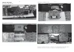
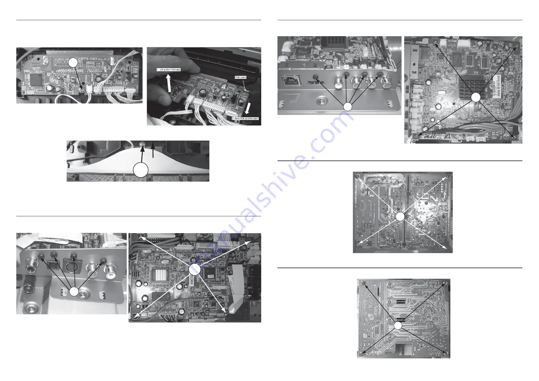
Dismantling of the Bd Board
1) Loosen 4 screws “O” as shown in fi gure 17.
2) Loosen 4 screws “P” on the top of BD Board as shown in fi gure 18.
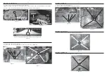
Dismantling of the VFD+LED Board
1) Loosen 1 screw “K” on the top of VFD Board as shown in fi gure 12.
2) Remove the VFD Board by lifting screw mounting side up and outwards from the 2 catches for the VFD Board as shown in Figure
13.
3) Loosen 1 screw “L” and according upward marking to slot out the Led Board as shown in fi gure 14.
Figure 12
Figure 13
Dismantling of the Main Board
1) Loosen 4 screws “M” as shown in fi gure 15.
2) Loosen 4 screws “N” on the top of Main Board as shown in fi gure 16 to remove Main Board.
Figure 14
Figure 15
Figure 16
Figure 19
K
M
N
L
Un-slot Led Board
Caution: Do not break the heat-sealed on both side of the white light guide
Figure 17
Dismantling of the Power Board
1) Loosen 4 screws “Q” on the bottom of Power Bard as shown in fi gure 19.
Q
P
Figure 18
Dismantling of the AMP Board
1) Loosen 4 screws “R” on the bottom of AMP Bard as shown in fi gure 20.
R
Figure 20
O
Summary of Contents for HTS9140/12
Page 10: ...2 3 2 3 REPAIR INSTRUCTIONS One ...
Page 16: ...4 3 4 3 9 AAA x 2 10 TV HDMI 1 HOME THEATER HOME THEATER 2 4 3 5 ...
Page 17: ...4 4 4 4 2 1 1 2 1 3 USB 2 0 Wi Fi 1 1 2 2 3 3 MP3 Link Cable ...
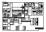
Page 20: ...5 1 5 1 BLOCK DIAGRAM ...
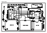
Page 21: ...5 2 5 2 WIRING DIAGRAM V5 V6 V12 V11 V4 V10 V9 V8 V7 V3 V2 V1 ...
Page 42: ...9 10 9 10 CIRCUIT DIAGRAM nine A 1 2 3 1 2 3 HA500 A3 ...
Page 45: ...9 13 9 13 CIRCUIT DIAGRAM twelve 1 2 3 1 2 3 A B C A B C R622 A1 R659 C2 R683 A1 R684 A1 ...
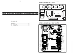
Page 48: ...10 1 10 1 TOUCH BOARD TABLE OF CONTENTS Circuit Diagram 10 2 PCB Layout Top Bottom View 10 3 ...
Page 57: ...12 3 12 3 Packing View for 93 only P1 Main Unit WLBRK WLSCR ...


