Circuit Description
9.
9.3
Video Signal Processing
9.3.1
Introduction
The video signal-processing path consists of the following
parts:
•
RF signal processing.
•
Video source selection.
•
Comb filter.
•
Video demodulation.
•
Luminance / Chrominance signal processing.
•
RGB control.
•
RGB amplifier
The processing circuits listed above are all integrated in the
UOC TV processor. The surrounding components are for the
adaptation of the selected application. The I
2
C bus is for
defining and controlling the signals.
9.3.2
RF Signal Processing
The incoming RF signal goes to the tuner (pos. 1000), where
the 45.75 MHz IF signal is developed and amplified. The IF
signals then exits the tuner from pin 11 to pass through the
SAW filter (pos. 1002/1003). The shaped signal is then applied
to the IF processor part of the UOC (pos. 7200).
Tuner AGC (Automatic Gain Control) will reduce the tuner gain
and thus the tuner output voltage when receiving strong RF
signals. Adjust the AGC takeover point via the Service Default
Alignment Mode (SDAM). The tuner AGC starts working when
the video-IF input reaches a certain input level and will adjust
this level via the I
2
C bus. The tuner AGC signal goes to the
tuner (pin 1) via the open collector output (pin 22) of the UOC.
The IC also generates an Automatic Frequency Control (AFC)
signal that goes to the tuning system via the I
2
C bus, to provide
frequency correction when needed.
The demodulated composite video signal is available at pin 38
and then buffered by transistor 7201.
9.3.3
Video Source Selection
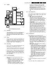
The Composite Video Blanking Signal (CVBS) from buffer
7201 goes to the audio carrier trap filters 1200, 1201, or 1202
(depending on the system used), to remove the audio signal.
The signal then goes to pin 40 of IC 7200. The internal input
switch selects the following input signals:
•
Pin 40: terrestrial CVBS input
•
Pin 42: external AV1 CVBS input
•
Pin 44: external Side I/O CVBS or AV2 (or comb filter)
luminance (Y) input
•
Pin 45: external AV2 (or comb filter) chrominance (C) input
Figure 9-3 Video source selection
Once the signal source is selected, a chroma filter calibration is
performed. The received color burst sub-carrier frequency is
used for this. Correspondingly, the chroma band pass filter for
PAL/NTSC processing or the cloche filter for SECAM
processing is switched on. The selected luminance (Y) signal
is supplied to the horizontal and vertical synchronization circuit
and to the luminance processing circuit. In the luminance-
processing block, the luminance signal goes to the chroma trap
filter. This trap is switched 'on' or 'off' depending on the color
burst detection of the chroma calibration circuit.
The group delay correction part can be switched between the
BG and a flat group delay characteristic. This has the
advantage that in multi-standard receivers no compromise has
to be made for the choice of the SAW filter.
9.3.4
Video Demodulation
The color decoder circuit detects whether the signal is a PAL,
NTSC, or SECAM signal. The result is made known to the auto
system manager. The PAL/NTSC decoder has an internal
clock generator, which is stabilized to the required frequency
by using the 12 MHz clock signal from the reference oscillator
of the microcontroller / teletext decoder.
The base-band delay line is used to obtain a good suppression
of cross color effects.
The Y signal and the delay line outputs U and V are applied to
the luminance / chroma signal processing part of the TV
processor.
9.3.5
Luminance / Chrominance signal Processing
The output of the YUV separator is fed to the internal YUV
switch, which switches between the output of the YUV
separator or the external YUV (for DVD or PIP) on pins 51-53.
Pin 50 is the input for the insertion control signal called 'FBL-1'.
When this signal level becomes higher than 0.9 V (but less than
3 V), the RGB signals at pins 51, 52, and 53 are inserted into
the picture by using the internal switches.
Also, some picture improvement features are implemented in
this part:
•
Black stretch. This function corrects the black level of
incoming signals, which have a difference between the
black level and the blanking level. The amount of extension
depends upon the difference between actual black level
and the darkest part of the incoming video signal level. It is
detected by means of an internal capacitor.
•
White stretch. This function adapts the transfer
characteristic of the luminance amplifier in a non-linear way
depending on the average picture content of the luminance
signal. It operates in such a way that maximum stretching
is obtained when signals with a low video level are
received. For bright pictures, stretching is not active.
•
Dynamic skin tone correction. This circuit corrects
(instantaneously and locally) the hue of those colors, which
are located in the area in the UV plane that matches the
skin tone. The correction is dependent on the luminance,
saturation, and distance to the preferred axis.
The YUV signal is then fed to the color matrix circuit, which
converts it to R, G, and B signals.
The OSD/TXT signal from the microprocessor is mixed with the
main signal at this point, before being output to the CRT board
(pins 56, 57, and 58).
9.3.6
RGB Control
The RGB control circuit enables the picture parameters
contrast, brightness, and saturation to be adjusted, by using a
combination of the user menus and the remote control.
Additionally automatic gain control for the RGB signals via cut-
off stabilization is achieved in this functional block to obtain an
accurate biasing of the picture tube. Therefore, this block
1,
12
2,
15
5,
14
FRONT
AUDIO
IN
AV1
AUDIO
IN
AV1
AUDIO
IN
7801
3,
13
7802
7901
47
30,
31
7831
CL
16532016_011.eps
120401
RGB/YUV
INSERT
RGB
56˜58
VIDEO
PROC.
AUDIO
AMPL.
42
7200
V-OUT
L/R
OUT
UOC
µP
CRT
PANEL
MON.
OUT
MAIN_OUT
24,25
SOUND
DEC
44
C-IN
45
SY_CVBS_IN
9
70
SEL-MAIN-FRNT-RR
QSS_AM_DEM_OUT
4
9
10
SC2-CTRL
40
AV1_CVBS1_1
51˜53
RGB/YUV
_IN
CVBS_FRONT_IN
0225-B
AV2
CVBS_IN
SVHS
Y_IN
C_IN
INTERNAL_CVBS_IN
41,
42
SC1-IN
47
Summary of Contents for L01.1L AC
Page 6: ...Directions for Use EN 6 L01 1L AC 3 3 Directions for Use 3 1 16 9 Sets ...
Page 7: ...Directions for Use EN 7 L01 1L AC 3 ...
Page 8: ...Directions for Use EN 8 L01 1L AC 3 ...
Page 9: ...Directions for Use EN 9 L01 1L AC 3 ...
Page 10: ...Directions for Use EN 10 L01 1L AC 3 ...
Page 11: ...Directions for Use EN 11 L01 1L AC 3 ...
Page 12: ...Directions for Use EN 12 L01 1L AC 3 ...
Page 13: ...Directions for Use EN 13 L01 1L AC 3 ...
Page 14: ...Directions for Use EN 14 L01 1L AC 3 ...
Page 15: ...Directions for Use EN 15 L01 1L AC 3 ...
Page 16: ...Directions for Use EN 16 L01 1L AC 3 Personal Notes ...
Page 17: ...Directions for Use EN 17 L01 1L AC 3 3 2 4 3 Sets Personal Notes ...
Page 42: ...Spare Parts List EN 82 L01 1L AC 10 10 Spare Parts List Not applicable yet ...
Page 43: ...Revision List EN 83 L01 1L AC 11 11 Revision List First release ...

