Circuit Description
9.
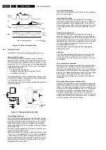
frequency of the line deflection coil and the S-correction
capacitors and therefore a less steep S-corrected line
deflection current.
9.6
Power Supply
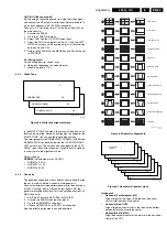
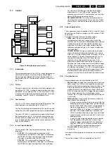
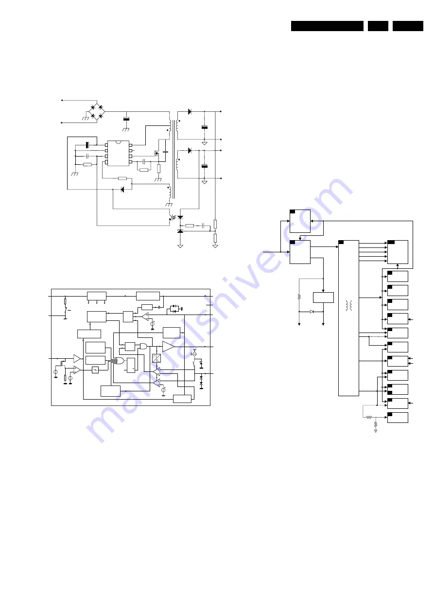
Figure 9-4 Switched Mode Power Supply standard circuit
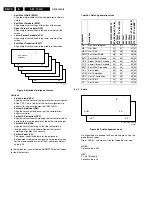
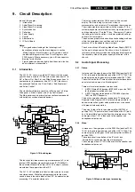
Figure 9-5 Internal block diagram of the driver IC (TEA1507)
9.6.1
Introduction
The supply is a Switching Mode Power Supply (SMPS). The
frequency of operation varies with the circuit load. This 'Quasi-
Resonant Flyback' behavior has some important benefits
compared to a 'hard switching' fixed frequency Flyback
converter. The efficiency can be improved up to 90%, which
results in lower power consumption. Moreover, the supply runs
cooler and safety is enhanced.
The power supply starts operating when a DC voltage goes
from the rectifier bridge via T5520, R3532 to pin 8. The
operating voltage for the driver circuit is also taken from the
'hot' side of this transformer.
The switching regulator IC 7520 starts switching the FET 'on'
and 'off', to control the current flow through the primary winding
of transformer 5520. The energy stored in the primary winding
during the 'on' time is delivered to the secondary windings
during the 'off' time.
The 'MainSupply' line is the reference voltage for the power
supply. It is sampled by resistors 3543 and 3544 and fed to the
input of the regulator 7540 / 6540. This regulator drives the
feedback optocoupler 7515 to set the feedback control voltage
on pin 3 of 7520.
The power supply in the set is 'on' any time AC power goes to
the set.
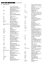
Derived Voltages
The voltages supplied by the secondary windings of T5520 are:
•
'MainAux' for the audio circuit (voltage depends on set
execution, see table below),
•
3.3 V and 3.9 V for the microprocessor and
•
'MainSupply' for the horizontal output (voltage depends on
set execution, see table below).
Other supply voltages are provided by the LOT. It su50
V (only for large screen sets), +13 V, +8 V, +5 V, and a +200 V
source for the video drive. The secondary voltages of the LOT
are monitored by the 'EHTinformation' lines. These lines are
fed to the video processor part of the UOC IC 7200 on pins 11
and 34.
This circuit will shut 'off' the horizontal drive in case of over-
voltage or excessive beam current.
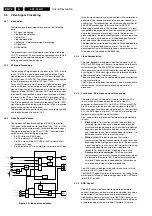
Figure 9-6 Derived voltages
Degaussing
When the set is switched on, the degaussing relay 1515 is
immediately activated as transistor 7580 is conducting. Due to
the RC-time of R3580 and C2580, it will last about 3 to 4
seconds before transistor 7580 is switched off.
9.6.2
Basic IC Functionality
For a clear understanding of the Quasi-Resonant behavior, it is
possible to explain it by a simplified circuit diagram (see Figure
below). In this circuit diagram, the secondary side is transferred
to the primary side and the transformer is replaced by an
inductance L_p. Capacitor C_d is the total drain capacitance
including the resonance capacitor C_r, parasitic output
capacitor C_oss of the MOSFET and the winding capacitance
C_w of the transformer. The turn ratio of the transformer is
represented by n (N_p/N_s).
Demag
4
Ctrl
Gnd
Vcc
Drain
HVS
Driver
Sense
3
2
1
5
6
7
8
V
LINE
V
TEA1507
IN
C
IN
V
CC
C
D
R
SENSE
C
SS
R
SS
V
OUT
N
S
N
P
N
Vcc
CL 16532020_074.eps
120401
SUPPLY
MANAGEMENT
internal
supply
UVLO
start
M-level
VCC
1
2
3
GND
S1
CTRL
FREQUENCY
CONTROL
VOLTAGE
CONTROLLED
OSCILLATOR
LOGIC
LOGIC
OVER-
VOLTAGE
PROTECTION
OVERPOWER
CL 16532020_073.eps
060701
PROTECTION
short
winding
soft
start
S2
OVER-
TEMPERATURE
PROTECTION
S
Q
R
UVLO
Q
MAXIMUM
ON-TIME
PROTECTION
POWER-ON
RESET
−
1
VALLEY
TEA1507
100 mV
clamp
DRIVER
START-UP
CURRENT SOURCE
0.75 V
0.5 V
5
Isense
6
DRIVER
4
DEM
8
DRAIN
7
HVS
n.c.
OCP
LEB
blank
Iss
2.5 V
burst
detect
CL 16532008_004.eps
250401
Tilt&
Rotation
A15
Lot
EHT
VG2
VideoSupply
Filament
Focus
A2
CRT
Panel
B1/B2
Main
Power
Supply
+3.9V
+3.3V
Degaussing
Circuit
A1
3V3 Reg.
A1
Degaussing
Control
Circuit
A1
EW
Correction
A2
Horizontal
Deflection
Vaux
+3.3V
+3.9V
Vaux
A2
Frame
Deflection
A3
Tuner
A4
uP
A7
Video
Processing
A5
Sound
Processing
A9
A11
Audio
Amplifier
+6.8V
A8
Source
Selection
Switch
A10
Main Supply
Mains AC
Input
Main Aux
V13V
VlotAux -13V
V5V
+8V
VT_Supply
*V50V
Summary of Contents for L01.1L AC
Page 6: ...Directions for Use EN 6 L01 1L AC 3 3 Directions for Use 3 1 16 9 Sets ...
Page 7: ...Directions for Use EN 7 L01 1L AC 3 ...
Page 8: ...Directions for Use EN 8 L01 1L AC 3 ...
Page 9: ...Directions for Use EN 9 L01 1L AC 3 ...
Page 10: ...Directions for Use EN 10 L01 1L AC 3 ...
Page 11: ...Directions for Use EN 11 L01 1L AC 3 ...
Page 12: ...Directions for Use EN 12 L01 1L AC 3 ...
Page 13: ...Directions for Use EN 13 L01 1L AC 3 ...
Page 14: ...Directions for Use EN 14 L01 1L AC 3 ...
Page 15: ...Directions for Use EN 15 L01 1L AC 3 ...
Page 16: ...Directions for Use EN 16 L01 1L AC 3 Personal Notes ...
Page 17: ...Directions for Use EN 17 L01 1L AC 3 3 2 4 3 Sets Personal Notes ...
Page 42: ...Spare Parts List EN 82 L01 1L AC 10 10 Spare Parts List Not applicable yet ...
Page 43: ...Revision List EN 83 L01 1L AC 11 11 Revision List First release ...

