Circuit Descriptions, Abbreviation List, and IC Data Sheets
9.
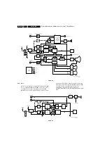
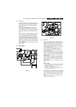
Figure 9-8
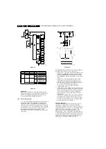
Figure 9-9
Degaussing
When the set is switched on, the degaussing relay 1515 is
immediately activated as transistor 7580 is conducting. Due to
the RC-time of R3580 and C2580, it will last about 3 to 4
seconds before transistor 7580 is switched off.
9.6.2
Basic IC Functionality
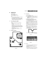
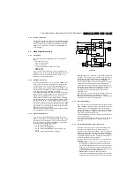
For a clear understanding of the Quasi-Resonant behaviour, it
is possible to explain it by a simplified circuit diagram (see
Figure below). In this circuit diagram, the secondary side is
transferred to the primary side and the transformer is replaced
by an inductance L
P
. C
D
is the total drain capacitance including
the resonance capacitor C
R
, parasitic output capacitor C
OSS
of
the MOSFET and the winding capacitance C
W
of the
transformer. The turns ratio of the transformer is represented
by n (N
P
/N
S
).
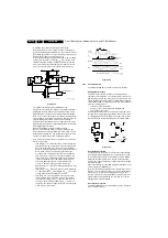
Figure 9-10
In the Quasi-Resonant mode each period can be divided into
four different time intervals, in chronological order:
•
Interval 1: t0 < t < t1 primary stroke At the beginning of the
first interval, the MOSFET is switched ‘on’ and energy is
stored in the primary inductance (magnetisation). At the
end, the MOSFET is switched ‘off’ and the second interval
starts.
•
Interval 2: t1 < t < t2 commutation time In the second
interval, the drain voltage will rise from almost zero to
V
IN
+n•(V
OUT
+V
F
). V
F
is the forward voltage drop of de
diode that will be omitted from the equations from now on.
The current will change its positive derivative,
corresponding to V
IN
/L
P
, to a negative derivative,
corresponding to -n•V
OUT
/L
P
.
•
Interval 3: t2 < t < t3 secondary stroke In the third interval,
the stored energy is transferred to the output, so the diode
starts to conduct and the inductive current I
L
will decrease.
In other words, the transformer will be demagnetised.
When the inductive current has become zero the next
interval begins.
•
Interval 4: t3 < t < t00 resonance time In the fourth interval,
the energy stored in the drain capacitor C
D
will start to
resonate with the inductance L
P
. The voltage and current
waveforms are sinusoidal waveforms. The drain voltage
will drop from V
IN
+n•V
OUT
to V
IN
-n•V
OUT
.
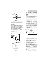
Frequency Behaviour
The frequency in the QR-mode is determined by the power
stage and is not influenced by the controller (important
parameters are L
P
and C
D
). The frequency varies with the input
voltage V
IN
and the output power P
OUT
. If the required output
power increases, more energy has to be stored in the
transformer. This leads to longer magnetising t
PRIM
and
demagnetising t
SEC
times, which will decrease the frequency.
See the frequency versus output power characteristics below.
The frequency characteristic is not only output power-, but also
input voltage dependent. The higher the input voltage, the
smaller t
PRIM
, so the higher the frequency will be.
CL 16532008_004.eps
250401
Tilt&
Rotation
A15
Lot
EHT
VG2
VideoSupply
Filament
Focus
A2
CRT
Panel
B1/B2
Main
Power
Supply
+3.9V
+3.3V
Degaussing
Circuit
A1
3V3 Reg.
A1
Degaussing
Control
Circuit
A1
EW
Correction
A2
Horizontal
Deflection
Vaux
+3.3V
+3.9V
Vaux
A2
Frame
Deflection
A3
Tuner
A4
uP
A7
Video
Processing
A5
Sound
Processing
A9
A11
Audio
Amplifier
+6.8V
A8
Source
Selection
Switch
A10
Main Supply
Mains AC
Input
Main Aux
V13V
VlotAux -13V
V5V
+8V
VT_Supply
*V50V
<>*'?'
/
/@
J'
K
J'*
Q
=4
>B%
*+
%%+
:&OF
=%:O&OO
Z\
#Z\
Z\
Z
=4:
>B
%"+
:%OF
=%:%O
%&"+
%*jF
!&&+
=4
>B%
%&+
)*j)RQ(
)RQ)&O
)RQ(OkRQO
%+
:%O&OO
''
^
=4:
>B
%"+
=%:%O
CL 16532008_0
6
3
2
3
0501
V
IN
V
GATE
V
D
n
⋅
V
OUT
I
L
C
D
C
OUT
D
L
P
C
IN
0
Demagneti-
zation
V
GATE
V
D
I
L
0
Magnetization
t
1
t
2
t
3
t
00
T
t
0
1
2
3
4
Valley
n
⋅
V
OUT
V
IN
CL 16532020_084.eps
110401

