Circuit Descriptions, Abbreviation List, and IC Data Sheets
9.
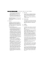
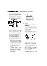
In Standby, the power supply works in ‘burst mode’.
Burst mode can be used to reduce the power consumption
below 1 W at stand-by. During this mode, the controller is active
(generating gate pulses) for only a short time and for a longer
time inactive waiting for the next burst cycle.
In the active period the energy is transferred to the secondary
and stored in the buffer capacitor C
STAB
in front of the linear
stabiliser (see Figure below). During the inactive period, the
load (e.g. microprocessor) discharges this capacitor. In this
mode, the controller makes use of the Safe-Restart mode.
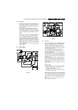
Figure 9-14
The system enters burst mode standby when the
microprocessor activates the ‘Stdby_con’ line. When this line is
pulled high, the base of Q7541 is allowed to go high. This is
triggered by the current from collector Q7542. When Q7541
turns ‘on’, the opto-coupler (7515) is activated, sending a large
current signal to pin 3 (Ctrl). In response to this signal, the IC
stops switching and enters a ‘hiccup’ mode. This burst
activation signal should be present for longer than the ‘burst
blank’ period (typically 30
µ
s): the blanking time prevents false
burst triggering due to spikes.
Burst mode standby operation continues until the
microcontroller pulls the ‘Stdby_con’ signal low again. The
base of Q7541 is unable to go high, thus cannot turn ‘on’. This
will disable the burst mode. The system then enters the start-
up sequence and begins normal switching behaviour.
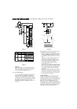
For a more detailed description of one burst cycle, three time
intervals are defined:
•
t1: Discharge of V
CC
when gate drive is active During the
first interval, energy is transferred, which result in a ramp-
up of the output voltage (V
STAB
) in front of the stabiliser.
When enough energy is stored in the capacitor, the IC will
be switched ‘off’ by a current pulse generated at the
secondary side. This pulse is transferred to the primary
side via the opto coupler. The controller will disable the
output driver (safe restart mode) when the current pulse
reaches a threshold level of 16 mA into the Ctrl pin. A
resistor R
1
(R3519) is placed in series with the opto
coupler, to limit the current going into the Ctrl pin.
Meanwhile the V
CC
capacitor is discharged but has to stay
above V
UVLO
.
•
t2: Discharge of V
CC
when gate drive is inactive During the
second interval, the V
CC
is discharged to V
UVLO
. The output
voltage will decrease depending on the load.
•
t3: Charge of V
CC
when gate drive is inactive The third
interval starts when the UVLO is reached. The internal
current source charges the V
CC
capacitor (also the soft
start capacitor is recharged). Once the V
CC
capacitor is
charged to the start-up voltage, the driver is activated and
a new burst cycle is started.
Figure 9-15
9.6.3
Protection Events
The SMPS IC 7520 has the following protection features:
Demagnetisation sense
This feature guarantees discontinuous conduction mode
operation in every situation. The oscillator will not start a new
primary stroke until the secondary stroke has ended. This is to
ensure that FET 7521 will not turn on until the demagnetisation
of transformer 5520 is completed. The function is an additional
protection feature against:
•
saturation of the transformer,
•
damage of the components during initial start-up,
•
an overload of the output.
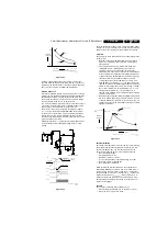
The demag(netisation) sense is realised by an internal circuit
that guards the voltage (Vdemag) at pin 4 that is connected to
V
CC
winding by resistor R
1
(R3522). The Figure below shows
the circuit and the idealised waveforms across this winding.
Figure 9-16
Over Voltage Protection
The Over Voltage Protection ensures that the output voltage
will remain below an adjustable level. This works by sensing
the auxiliary voltage via the current flowing into pin 4 (DEM)
during the secondary stroke. This voltage is a well-defined
replica of the output voltage. Any voltage spikes are averaged
by an internal filter.
If the output voltage exceeds the OVP trip level, the OVP circuit
switches the power MOSFET ‘off’.
Next, the controller waits until the ‘under voltage lock out‘ level
(UVLO =
±
9 V) is reached on pin 1 (V
CC
). This is followed by a
safe restart cycle, after which switching starts again. This
process is repeated as long as the OVP condition exists. The
output voltage at which the OVP function trips, is set by the
demagnetisation resistor R3522.
Over Current Protection
The internal OCP protection circuit limits the ‘sense’ voltage on
pin 5 to an internal level.
Demag
4
Ctrl
Gnd
Vcc Drain
HVS
Driver
Sense
3
2
1
5
6
7
8
Burst-Mode stand-by on/off
from microprocessor
Linear
stabilizer
V
STAB
V
µ
C
C
STAB
C
Vcc
V
CC
R
1
Current pulse
generator
V
IN
Basic Burst mode configuration
CL 16532020_081.eps
100401
V
(start)
V
(UVLO)
V
CC
V
STAB
I
L
Active/
inactive
t1
t2
t3
V
µ
C
Soft start
Burst mode waveforms
CL 16532020_082.eps
100401
R
1
R
2
D
V
CC
winding
I
(ovp)(demag)
I
(opp)(demag)
Demag
4
Ctrl
Gnd
Vcc
Drain
HVS
Driver
Sense
3
2
1
5
6
7
8
configuration
A
B
0V
OUT
S
Vcc
V
N
N
⋅
IN
P
Vcc
V
N
N
⋅
Demagnetization
V
GATE
V
WINDING
Magnetization
V
demag
Comparator
threshold
V
demag
0.7V
0V
-0.25V


